Introduction
In high-speed PCB design, signal integrity represents a critical factor that determines whether a board delivers reliable performance or succumbs to subtle failures. Engineers often face the signal integrity gamble when selecting PCB size, as larger dimensions provide routing flexibility but introduce propagation delays and distortion risks, while compact layouts demand precision to avoid density-related issues. PCB size and signal integrity become intertwined challenges, especially at data rates exceeding several gigabits per second, where signals behave as electromagnetic waves rather than simple DC paths. This article delves into how board dimensions influence impedance control, exacerbate signal reflection issues, and complicate minimizing signal distortion. By understanding these relationships, designers can make informed choices that balance functionality, manufacturability, and performance. Ultimately, mastering these aspects ensures robust high-speed PCB design outcomes.
Understanding Signal Integrity in the Context of PCB Size
Signal integrity refers to the preservation of electrical signal quality from source to receiver, encompassing amplitude, timing, and shape fidelity. In high-speed environments, factors like crosstalk, attenuation, and reflections degrade signals, leading to bit errors or system instability. PCB size plays a pivotal role because it dictates trace lengths, layer stacking, and mechanical stability, all of which impact wave propagation. Larger boards allow for distributed components and power planes but amplify losses over distance, whereas smaller ones concentrate signals, heightening coupling effects. This dynamic turns PCB size into a strategic decision, where overlooking its implications can undermine even the most optimized layouts. Industry relevance stems from rising demands in telecommunications, computing, and automotive electronics, where high-speed interfaces like PCIe or DDR dominate.
The interplay begins with transmission line theory, treating traces as controlled-impedance paths. Characteristic impedance depends on trace width, thickness, dielectric height, and material properties, but board size affects uniformity across the panel. For instance, expansive designs risk variations in dielectric constant due to fabrication tolerances, altering signal velocity. Engineers must weigh these against enclosure constraints and thermal management, as oversized boards may require segmentation to maintain integrity. Why it matters: poor signal integrity cascades into EMI compliance failures, higher power consumption from retransmissions, and costly respins. Addressing PCB size and signal integrity early in the design cycle thus safeguards project timelines and budgets.
Core Mechanisms: How PCB Dimensions Drive Signal Integrity Challenges
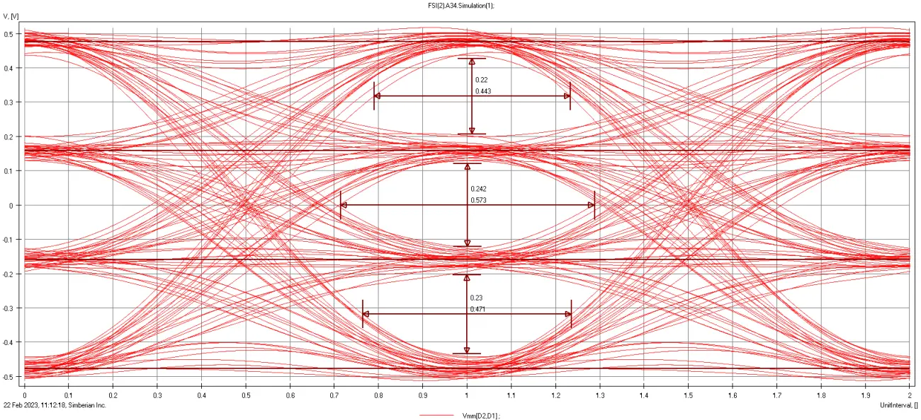
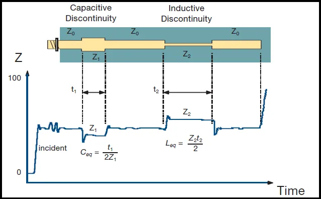
At the heart of high-speed PCB design lies transmission line behavior, where trace length relative to signal wavelength determines if lumped or distributed models apply. On larger PCBs, traces often exceed a significant fraction of the wavelength, say at 10 Gb/s where lambda is around 15 mm in FR-4, leading to phase shifts and ringing. This extends rise times artificially, closing eye openings and reducing margins. Signal reflection issues arise primarily from impedance discontinuities, such as vias, bends, or connectors, which are harder to minimize over extended routes. Reflection coefficient Gamma quantifies this mismatch, where even small deviations from 50 ohms or 100 ohms differential cause voltage overshoots. Larger boards compound the problem by necessitating more vias for layer transitions, each introducing stubs that reflect energy back.
Dielectric and conductor losses scale with distance, manifesting as attenuation that high-frequencies suffer most due to skin effect and dispersion. In compact designs, parallel routing density spikes crosstalk, with near-end and far-end coupling distorting victim signals via capacitive and inductive mechanisms. PCB size influences stackup feasibility; thicker boards for rigidity in large formats separate signals better but increase via lengths, worsening reflections. Mechanical factors like warpage further perturb impedance by varying dielectric spacing, a concern amplified in oversized panels during lamination or reflow. Per IPC-2141A guidelines for controlled impedance, maintaining tolerance across varying dimensions requires precise material selection and process controls. These mechanisms underscore why PCB size demands rigorous simulation before fabrication.
Crosstalk mechanisms intensify with board scale. Aggressive coupling occurs when aggressor traces switch nearby victims, injecting noise proportional to length and proximity. Large PCBs permit serpentine routing for length matching, but this curls increase self-inductance and radiation. Ground bounce and power integrity tie in, as expansive planes exhibit inductance at high frequencies, drooping supplies under simultaneous switching. Signal distortion accumulates from these, including inter-symbol interference where prior bits smear into successors. Minimizing signal distortion thus hinges on size-aware routing topologies, like orthogonal orientations or shielding. Warpage, bowing up to allowable limits under IPC-6012 specifications, subtly shifts trace-to-plane distances, detuning Z0 by percentages that matter at multi-GHz speeds.
Practical Best Practices for Mitigating Size-Related Risks
Effective high-speed PCB design starts with stackup optimization tailored to board dimensions. For larger PCBs, symmetric builds with balanced copper distribution control warpage and ensure uniform dielectric thickness for impedance control. Specify trace widths and spacings via field solvers to hit Z0 targets, accounting for fabrication tolerances like etch factor. Length tuning equalizes delays on clocks and data lines, crucial for setups like memory buses where skew exceeds timing budgets on long routes. Employ back-drilled vias to stub lengths below quarter-wave, reducing reflections in multi-layer large boards. Guard traces or moats isolate sensitive nets, curbing crosstalk in dense regions of any size.
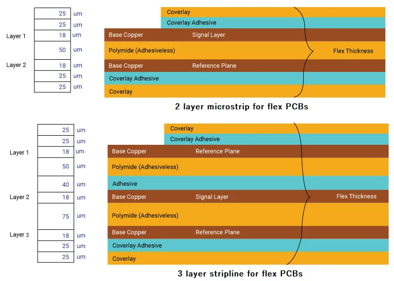
Material choice influences outcomes profoundly. Low-loss dielectrics with stable Dk minimize dispersion over distance, vital for expansive designs. Prepreg and core uniformity prevents Z0 gradients across the panel. Routing strategies adapt to size: microstrip for top layers on small boards, stripline buried for noise immunity on large ones. Simulate pre-layout with 3D solvers for S-parameters, validating return loss below -20 dB. Per IPC-2221 standards, incorporate test coupons for TDR verification post-fab, confirming impedance across the board. Decoupling caps placed strategically combat ground bounce, with via fencing enhancing return paths.
Fabrication liaison ensures tolerances align with design. Specify panel utilization to avoid edge effects in large formats, where copper imbalance warps. Assembly considerations include reflow profiles that exacerbate bow in oversized boards. Troubleshooting employs oscilloscopes for eye patterns and VNA for insertion loss, pinpointing size-induced anomalies. For segmentation in mega-boards, use high-speed connectors with matched Z0 and minimal skew. These practices, grounded in engineering rigor, transform the signal integrity gamble into a calculated win.
Troubleshooting Insights: Diagnosing Size-Induced SI Failures
Engineers encounter symptoms like jitter on receivers or intermittent data errors, often tracing to PCB size effects. Long traces show dispersive tails in scopes, while TDR spikes reveal via stubs. Crosstalk manifests as glitches on quiet lines during burst activity. Warpage suspicions arise from inconsistent performance across the board, confirmed via optical comparators. Differential pairs skew from unequal lengths, visible in bathtubs. Logical diagnosis sequences: review stackup for Z0 variance, resimulate with fab data, then proto-test.
A common pitfall in large PCBs is unaccounted enclosure resonances coupling to traces. Mitigation involves ground stitching and cavity shielding. Compact boards suffer pad density overwhelming drill capacities, spiking inductance. Iterative fixes include fanouts and blind vias. These insights, drawn from design cycles, highlight proactive size planning.
Conclusion
PCB size profoundly shapes signal integrity in high-speed designs, with larger formats risking attenuation and reflections, while smaller ones amplify crosstalk and density woes. Key to success lies in impedance control through stackups, routing discipline, and standards like IPC-2141A and IPC-6012. By anticipating mechanisms like warpage and loss, engineers minimize signal distortion via simulation and verification. This balanced approach turns gambles into guarantees, enabling reliable performance across scales. Prioritize these principles for future-proof high-speed PCB design.
FAQs
Q1: How does PCB size affect signal integrity in high-speed PCB design?
A1: PCB size influences signal integrity by altering trace lengths and densities; larger boards increase attenuation and reflection risks over distance, while smaller ones heighten crosstalk from tight routing. Engineers must optimize stackups for uniform impedance control and use length matching to preserve timing. Simulations predict these effects early, ensuring margins at gigabit speeds. Standards guide fabrication tolerances to maintain performance.
Q2: What are the main signal reflection issues caused by larger PCB sizes?
A2: Signal reflection issues in larger PCBs stem from extended trace paths and more vias, creating impedance mismatches that bounce energy back. Discontinuities like bends or stubs amplify Gamma, degrading eye quality. Back-drilling and controlled etching mitigate this, per industry guidelines. TDR testing verifies fixes post-fabrication.
Q3: How can engineers achieve impedance control regardless of PCB size?
A3: Impedance control relies on precise trace geometry, dielectric spacing, and material stability, scalable to any size via field calculators. Symmetric stackups prevent warpage-induced variations, ensuring Z0 tolerance. Include coupons for fab validation. This approach upholds high-speed PCB design integrity universally.
Q4: What strategies minimize signal distortion related to PCB dimensions?
A4: To minimize signal distortion, employ low-loss materials, orthogonal routing, and shielding against coupling, adapting to board scale. Equalize lengths and optimize vias for minimal stubs. Pre- and post-layout S-parameter analysis confirms low insertion loss and return loss.
References
IPC-2141A - Design Guide for High-Speed Controlled Impedance. IPC.
IPC-2221B - Generic Standard on Printed Board Design. IPC.
IPC-6012E - Qualification and Performance Specification for Rigid Printed Boards. IPC, 2017.


