Introduction
In high-speed PCB designs, maintaining signal integrity poses significant challenges as data rates continue to increase. Controlled impedance PCB traces ensure that signals propagate without distortion, reflections, or loss, which is essential for applications like telecommunications, computing, and automotive electronics. Layer thickness plays a pivotal role in this process, directly influencing the characteristic impedance of transmission lines embedded within the PCB stackup. Engineers must carefully control PCB layer thickness impedance to achieve precise impedance matching across multiple layers. This article explores the engineering principles behind layer thickness effects, practical design strategies, and best practices for reliable performance. By understanding these relationships, designers can optimize their PCB stackup impedance for robust operation.
What Is Controlled Impedance and Why Does It Matter?
Controlled impedance refers to the consistent characteristic impedance of PCB traces, typically targeted at values like 50 ohms or 100 ohms for single-ended or differential pairs. This consistency prevents signal reflections that arise from impedance mismatches, which can degrade performance in high-frequency circuits. Transmission line impedance is governed by the geometry of the trace and the surrounding dielectric materials, making precise control critical for modern electronics.
In practice, impedance mismatches lead to issues such as crosstalk, timing skew, and bit errors in digital systems. For electric engineers working on multilayer boards, achieving controlled impedance PCB designs ensures compliance with signal integrity requirements. The relevance intensifies with rising edge speeds, where even minor variations can cause failures. Layer thickness emerges as a key parameter because it determines the distance between signal traces and reference planes, directly impacting capacitance and thus impedance.
PCB stackup impedance control becomes non-negotiable in dense, high-layer-count boards used in servers or RF modules. Without it, engineers face iterative redesigns and costly respins. Industry standards like IPC-2141A provide guidelines for designing these controlled environments, emphasizing the need for tight tolerances.
Technical Principles of Layer Thickness in Impedance Control
The characteristic impedance of a transmission line, Z0, derives from the ratio of inductance per unit length to capacitance per unit length, expressed as Z0 equals the square root of L over C. In PCBs, capacitance C increases as the dielectric thickness between a signal trace and its reference plane decreases, since closer conductors store more electric field energy. Consequently, thinner layers result in lower impedance for a given trace width, while thicker layers raise impedance by reducing capacitance.
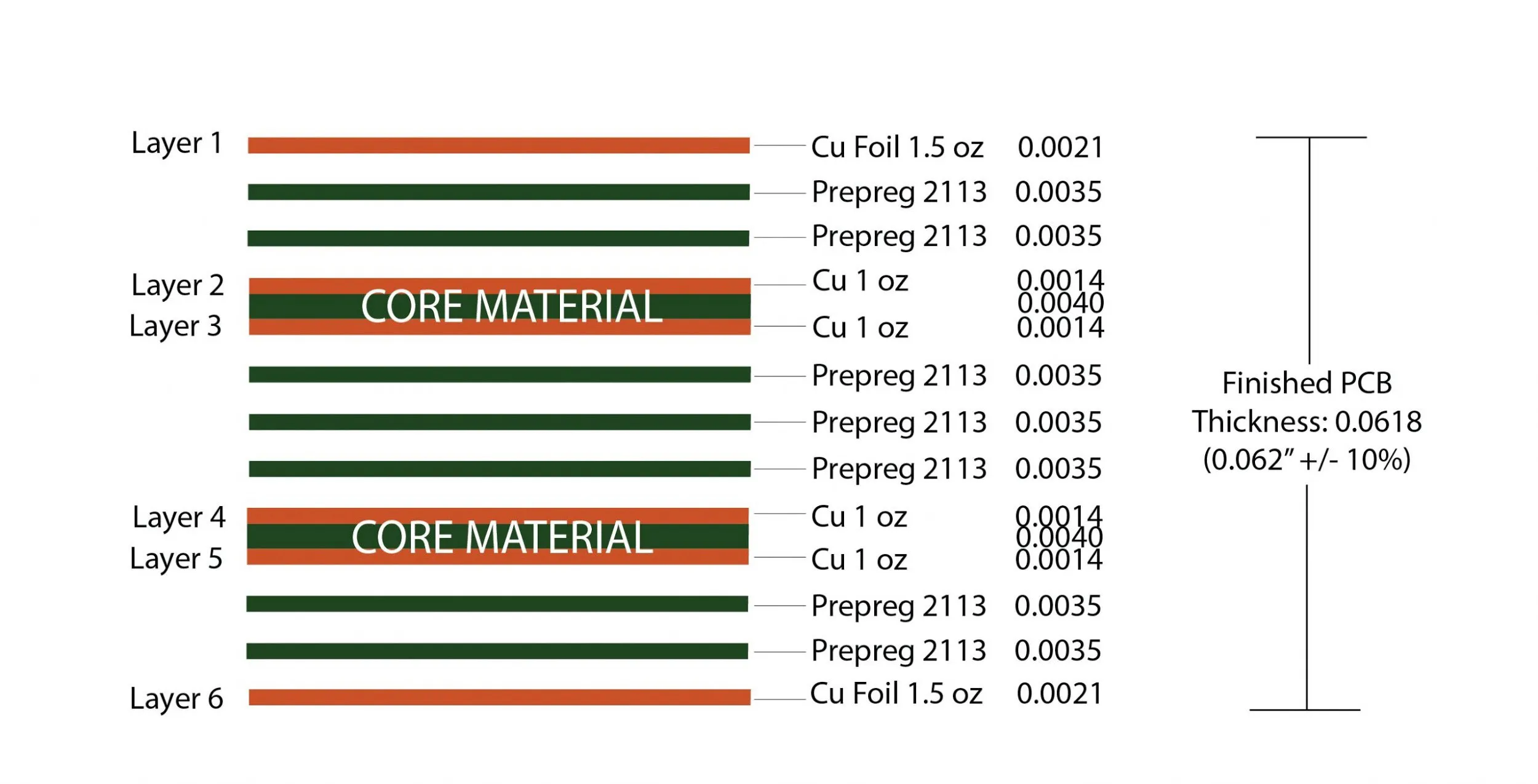
For microstrip lines on outer layers, the dielectric thickness is the full board height from trace to the nearest plane, often comprising core and prepreg materials. Striplines, embedded between two reference planes, depend on the symmetric dielectric thicknesses above and below the trace. Variations in these thicknesses alter the effective dielectric constant and field distribution, shifting Z0 predictably. Engineers model this using field solvers that account for PCB layer thickness impedance relationships.
Material properties like dielectric constant Er further modulate the effect, but layer thickness often dominates due to manufacturing sensitivities. IPC-2141A outlines calculation methods for these configurations, recommending empirical adjustments for real-world asymmetries. As frequency rises into gigahertz ranges, skin effect and surface roughness add complexities, but thickness remains foundational.
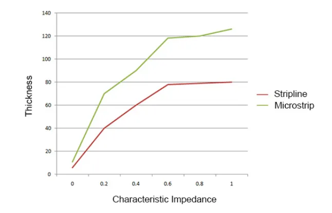
Transmission line impedance calculations reveal inverse proportionality: doubling dielectric thickness can increase Z0 by 20 to 30 percent, depending on geometry. This sensitivity necessitates precise stackup definitions early in design. Asymmetric stackups exacerbate issues, as outer layers experience air-dielectric interfaces that lower effective Er compared to internal striplines.
Factors Influencing Impedance Through Layer Thickness
Beyond basic geometry, manufacturing processes introduce variables like prepreg flow and resin content, which affect final cured thickness. Core thicknesses are more stable, sourced from laminate suppliers with tight specs, while prepregs compress during lamination, altering interlayer spacing. Engineers must predict these changes to hit target impedance matching.
Copper thickness also interacts, as thicker foils reduce effective trace height and slightly lower Z0, but layer dielectric dominates. Solder mask over outer traces adds a thin dielectric layer, typically dropping impedance by a few ohms. Comprehensive stackup planning integrates all these for holistic PCB stackup impedance control.
Temperature and humidity during fabrication influence resin cure, potentially varying thickness by percentages that translate to ohm shifts. Standards like IPC-6012E specify qualification tests verifying layer thickness uniformity post-fabrication.
Practical Solutions and Best Practices for Impedance Control
Designers start with stackup planning, defining layer count, material types, and target thicknesses to meet impedance specs across signal layers. Symmetric stackups minimize warpage and ensure consistent dielectric heights, facilitating uniform transmission line impedance. Specify tolerances tightly, such as plus or minus 10 percent on dielectric thickness, to limit Z0 variation to plus or minus 10 percent.
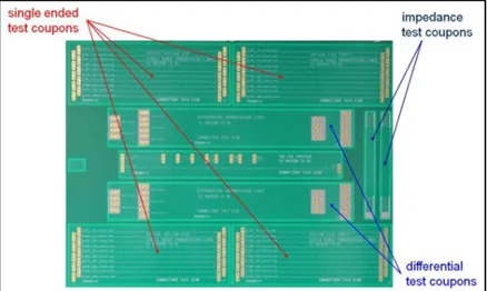
Collaborate with fabricators early, providing impedance worksheets detailing trace type, target Z0, and locations. Use controlled impedance coupons on panels for test coupons measured via time domain reflectometry. This verifies PCB layer thickness impedance before full production.
For multilayer boards, alternate signal and plane layers to provide low-inductance returns, enhancing impedance stability. Thinner dielectrics suit high-density designs needing lower Z0, but demand finer trace widths, increasing etch tolerances. Balance mechanical rigidity with electrical needs by mixing core and prepreg thicknesses judiciously.
Material selection favors low-loss dielectrics with stable Er, but prioritize those with predictable thickness control. Simulate stackups iteratively, correlating models with fab data for accuracy. Post-design, review fab drawings for thickness callouts matching your intent.
Troubleshooting Common Layer Thickness Issues
Deviations often stem from prepreg squeeze-out, where excess resin flows, thinning layers unexpectedly. Measure incoming laminates and simulate press cycles to anticipate this. Warped panels from asymmetric thicknesses disrupt parallelism, varying local impedances.
TDR traces revealing steps indicate thickness inconsistencies between nets. Cross-section analysis confirms root causes, guiding process tweaks. IPC-6012E acceptance criteria help qualify fixes.
High-frequency losses amplify thickness errors, as mode conversions occur. Differential pairs demand matched thicknesses for intra-pair balance.
Conclusion
Layer thickness profoundly shapes controlled impedance PCB performance, dictating capacitance and Z0 in transmission lines. Through principled stackup design, tight tolerances, and verification, engineers achieve reliable impedance matching. Adhering to guidelines in IPC-2141A ensures manufacturability and signal integrity. Prioritizing PCB layer thickness impedance from concept to production minimizes risks in high-speed applications. Future designs will leverage even tighter controls as frequencies climb.
FAQs
Q1: What is the impact of PCB layer thickness on controlled impedance?
A1: PCB layer thickness directly affects dielectric spacing, altering capacitance and thus transmission line impedance. Thinner layers lower impedance by increasing capacitance, while thicker ones raise it. Engineers adjust trace widths accordingly for target Z0, typically maintaining tolerances to ensure consistency across the stackup. This principle underpins reliable high-speed signal propagation.
Q2: How does PCB stackup impedance influence signal integrity?
A2: PCB stackup impedance determines reflection coefficients at transitions, critical for impedance matching. Poor control leads to ringing, overshoot, and eye closure in high-speed links. Proper layer thickness planning with reference planes minimizes these, supporting data rates beyond 10 Gbps. Verification via coupons confirms design intent.
Q3: Why is layer thickness critical for impedance matching in multilayer PCBs?
A3: In multilayer PCBs, layer thickness variations disrupt uniform field distribution, causing Z0 mismatches between layers. Symmetric stackups and precise prepreg selection mitigate this for consistent transmission line impedance. Fabricators target tolerances per standards to deliver matched performance, essential for RF and digital circuits.
Q4: What best practices ensure controlled impedance PCB fabrication?
A4: Define stackup with explicit thickness specs, simulate impedances, and include test structures. Communicate tolerances to fabs, expecting TDR validation. Symmetric designs aid uniformity, while material choices support low variation. This workflow achieves robust PCB layer thickness impedance control.
References
IPC-2141A — Design Guide for High-Speed Controlled Impedance Circuit Boards. IPC, 2009
IPC-6012E — Qualification and Performance Specification for Rigid Printed Boards. IPC, 2017
IPC-6012DS — Qualification and Performance Specification for Rigid Printed Boards with Embedded Components. IPC, 2015


