Introduction
Thermal runaway represents a critical failure mode in electronic systems where excessive heat generation exceeds dissipation capabilities, leading to accelerating temperature increases and potential component destruction. In maximum-sized PCBs, which push the limits of panel dimensions to accommodate complex circuitry, heat dissipation in large PCBs becomes particularly challenging due to extended thermal paths and uneven heat spreading. Engineers must prioritize PCB thermal management from the initial design phase to prevent such catastrophic events. This article explores the principles behind thermal runaway, its implications for large boards, and proven strategies like thermal vias and component placement for cooling. By adhering to established guidelines, designers can ensure reliable performance under high-power conditions. Effective heat management not only extends product lifespan but also maintains operational integrity in demanding applications.
What Is Thermal Runaway and Why It Matters in Large PCBs
Thermal runaway occurs when a device's junction temperature rises uncontrollably, often triggered by power dissipation that overwhelms cooling mechanisms, causing resistance changes that generate even more heat. In PCBs, this phenomenon typically starts at high-power components like power amplifiers or voltage regulators and can propagate across the board if not contained. For maximum-sized PCBs, the scale amplifies risks because heat must travel farther to reach edges or sinks, increasing the likelihood of localized hotspots. Industry standards such as IPC-2221 provide foundational guidelines for designing boards that mitigate these risks through proper material selection and layout. Poor management leads to delamination, solder joint failures, and system downtime, making preventing overheating in PCBs a non-negotiable priority for electric engineers. Understanding these dynamics ensures designs meet performance demands without compromising safety.
Mechanisms of Heat Generation and Dissipation in PCBs
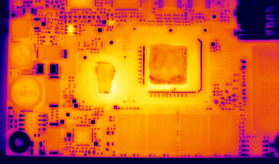
Heat in PCBs arises primarily from Joule heating in conductors, dielectric losses, and component power dissipation, with traces carrying high currents contributing significantly to overall board temperature. In large PCBs, conduction through copper layers dominates initial heat transfer, but convection and radiation play larger roles as board size increases due to greater surface area exposure to ambient air. Thermal resistance, quantified as the temperature difference per unit power, governs how effectively heat moves from sources to sinks. Factors like board thickness, layer count, and copper weight influence this resistance, with thicker boards offering better spreading but higher via thermal impedance. Engineers must model these paths accurately to predict hotspots. In maximum-sized configurations, uneven airflow across expansive surfaces can exacerbate imbalances, underscoring the need for strategic heat dissipation in large PCBs.
Challenges Specific to Maximum-Sized PCBs
Maximum-sized PCBs, often spanning full panel extents, face unique thermal hurdles from their sheer scale, including prolonged heat conduction distances that elevate internal temperatures. Fabrication constraints limit copper thickness uniformity over large areas, potentially creating weak points in thermal conductivity. Component density varies across the board, concentrating heat in central regions while edges benefit from natural convection. Mechanical stresses from thermal expansion mismatch further complicate dissipation, risking warpage or cracks. Airflow patterns in enclosures may bypass inner sections, intensifying the challenge of preventing overheating in PCBs. These factors demand a holistic approach to PCB thermal management tailored to oversized designs.
Best Practices for Component Placement for Cooling
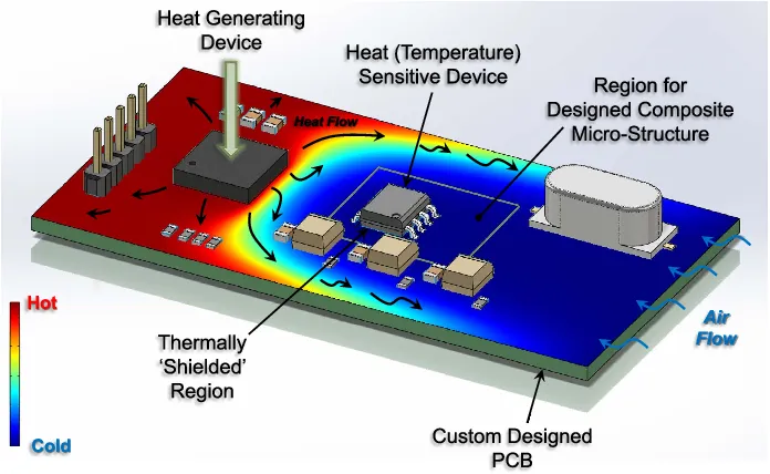
Optimal component placement for cooling begins with positioning high-heat generators near board edges or mounting points where heatsinks or fans can access them directly. Spacing sensitive analog or RF components away from power devices minimizes thermal crosstalk, preserving signal integrity. Grouping similar thermal profiles together allows targeted cooling zones, while avoiding clusters that form hotspots. In large PCBs, orienting components to align with expected airflow directions enhances convection efficiency. Vertical stacking via through-hole designs can sometimes aid vertical heat escape, but surface-mount preferences require careful pad planning. This strategy integrates seamlessly with broader PCB thermal management efforts.
Leveraging Thermal Vias for Effective Heat Transfer
Thermal vias serve as vertical conduits that shuttle heat from surface components to inner copper planes or the opposite side, drastically reducing thermal resistance in multilayer boards. Arrays of 0.3 mm diameter vias under hotspots, filled or tented to prevent solder wicking, provide low-impedance paths without compromising electrical isolation. In maximum-sized PCBs, distributing via farms strategically prevents board-wide temperature gradients. Plating thickness and spacing follow design rules to balance thermal conductance with fabrication yield. Combining vias with ground pours amplifies spreading. IPC-2152 offers insights into trace heating that complement via usage for comprehensive heat dissipation in large PCBs.
Material Selection and Layer Stackup Strategies
Selecting laminates with high glass transition temperatures supports thermal stability, while increasing copper weight in power planes boosts in-plane conduction. Multilayer stackups dedicate inner layers as thermal highways, sandwiching signal layers between them for shielding and dissipation. Varying core and prepreg thicknesses optimizes vertical heat flow. For large PCBs, symmetric stackups mitigate warpage from differential expansion. Heavier copper on outer layers aids surface convection. These choices form the backbone of preventing overheating in PCBs.
Simulation and Testing for Validation
Finite element analysis simulates steady-state and transient thermal profiles, revealing hotspots before prototyping. Boundary conditions mimic real-world airflow and component powers accurately. Iterative refinement adjusts layouts based on junction temperature predictions. Physical testing with thermocouples or IR cameras validates models under load. Standards like those in the JEDEC JESD51 series guide board-level thermal characterization. This validation loop ensures heat dissipation in large PCBs meets operational margins.
Advanced Techniques for Heat Dissipation
Copper pours and polygons under components create expansive heat spreaders, linking to vias for three-dimensional dissipation. Embedded heat pipes or vapor chambers suit extreme cases in large boards, though integration adds complexity. Board stiffeners double as heat bridges to chassis grounds. Active cooling via embedded fans targets persistent hotspots. Hybrid approaches combine passive and active elements judiciously.
Troubleshooting Common Thermal Issues
Hotspots persisting despite vias often stem from inadequate via density or plating; increasing arrays or tenting resolves this. Uneven heating across large PCBs signals poor plane connectivity, fixed by stitching vias. Component failures trace to underestimating derating factors. Warpage from thermal cycling requires balanced stackups. Systematic logging during testing pinpoints root causes efficiently.
Conclusion
Managing thermal runaway in maximum-sized PCBs demands a multifaceted approach centered on PCB thermal management principles. Strategic component placement for cooling, thermal vias, and robust stackups form the core defenses against overheating. Adhering to IPC-2221 and IPC-2152 ensures designs withstand real-world stresses. Engineers who integrate simulation, material savvy, and validation achieve reliable heat dissipation in large PCBs. Proactive strategies not only prevent failures but elevate overall system performance. Prioritizing these practices positions designs for success in high-stakes environments.
FAQs
Q1: What role do thermal vias play in PCB thermal management?
A1: Thermal vias enhance heat dissipation in large PCBs by providing low-resistance paths from surface components to inner layers or the board underside. Engineers place them in arrays under hotspots to distribute heat evenly, reducing junction temperatures. Proper sizing and density prevent electrical shorts while maximizing conductance. This technique proves essential for preventing overheating in PCBs, especially in multilayer maximum-sized boards. Follow design guidelines for optimal performance.
Q2: How does component placement for cooling impact heat dissipation in large PCBs?
A2: Component placement for cooling involves locating power devices near edges for sink access and spacing them from sensitive parts to curb crosstalk. In maximum-sized PCBs, alignment with airflow optimizes convection. This reduces thermal gradients and hotspots effectively. PCB thermal management improves reliability through such layouts. Simulations confirm placements before fabrication.
Q3: What are key strategies for preventing overheating in PCBs?
A3: Preventing overheating in PCBs relies on thermal vias, copper planes, and high-conductivity materials to spread heat. Multilayer designs dedicate planes for conduction, while edge placement aids convection. Validation via thermal profiling catches issues early. These practices align with industry benchmarks for robust heat dissipation in large PCBs. Consistent application ensures long-term stability.
Q4: Why is IPC-2152 relevant to thermal runaway prevention?
A4: IPC-2152 guides trace width selection based on current to limit heating, directly addressing precursors to thermal runaway. It accounts for board parameters like thickness and temperature rise in large PCBs. Engineers use it to size conductors avoiding excessive resistance buildup. This standard integrates with overall PCB thermal management for safe designs.
References
IPC-2221 — Generic Standard on Printed Board Design. IPC
IPC-2152 — Standard for Determining Current Carrying Capacity in Printed Board Design. IPC
JEDEC JESD51 — Integrated Circuits Thermal Test Method Environmental Conditions - Natural Convection (Still Air). JEDEC


