Introduction
In modern PCB design, achieving optimal electrical, thermal, and mechanical performance demands precise techniques that address multilayer challenges. Via stitching PCB and copper balancing emerge as complementary strategies, where via stitching connects separated ground plane sections for enhanced continuity, and copper balancing ensures uniform copper distribution across layers to mitigate stresses. This symbiotic relationship delivers ground plane improvement PCB by providing low-impedance return paths, supports impedance control PCB through consistent dielectric environments, and facilitates EMI reduction PCB via better shielding. Engineers often overlook their interplay, yet integrating both yields superior signal integrity and reliability in high-speed applications. As board complexity rises with denser components and faster signals, these methods become indispensable for maintaining performance margins. This article explores their principles, benefits, and implementation to guide electric engineers in leveraging their full potential.
Understanding Via Stitching in PCBs
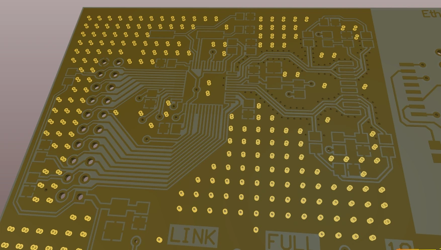
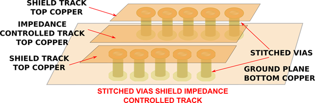
Via stitching PCB refers to the strategic placement of multiple vias in a pattern to electrically connect disjointed sections of copper planes, typically ground or power planes, across different layers. This technique creates redundant, low-inductance paths that distribute return currents evenly, reducing voltage drops and hotspots. Without stitching, isolated plane sections can lead to impedance discontinuities, exacerbating signal reflections in high-frequency designs. It also aids thermal management by providing additional paths for heat dissipation from components to inner layers. Compliance with IPC-2221B guidelines ensures stitching aligns with design rules for via size, spacing, and density to avoid fabrication issues. Overall, via stitching transforms fragmented planes into a unified shield, foundational for robust PCB operation.
Copper Balancing: Principles and Necessity
Copper balancing benefits arise from equalizing the copper coverage area on opposite sides of a PCB core or prepreg to prevent mechanical warpage during fabrication and assembly processes. Uneven copper distribution induces differential thermal expansion, causing bow and twist that compromise solder joint reliability and component alignment. Engineers calculate balance by matching the percentage of copper fill on each layer pair, often targeting within 10% variance though exact thresholds depend on stackup. This practice stabilizes the board's response to lamination temperatures and reflow profiles, preserving flatness critical for automated assembly. Copper balancing also indirectly supports electrical performance by maintaining uniform dielectric thickness, which influences characteristic impedance. In essence, it forms the mechanical backbone that enables other electrical optimizations.
The Symbiotic Interplay Between Via Stitching and Copper Balancing
Via stitching and copper balancing exhibit a symbiotic relationship where each enhances the other's effectiveness in multilayer boards. Stitching vias add copper-filled barrels that contribute to overall copper density, potentially unbalancing layers if not accounted for during pour adjustments. Conversely, balanced copper planes provide a stable substrate for stitching patterns, ensuring vias maintain electrical integrity without mechanical distortion from warpage. This duo optimizes ground plane improvement PCB by combining stitching's current-sharing with balancing's uniformity, minimizing loop inductance. For impedance control PCB, balanced layers preserve consistent trace-to-plane spacing, while stitching suppresses resonances. EMI reduction PCB benefits from the shielded enclosure formed by stitched, balanced planes, containing emissions effectively.
Technical Mechanisms Driving Performance Gains
Ground plane improvement PCB through via stitching begins with reducing partial ground inductance. In high-current scenarios, currents concentrate on the shortest paths to components, creating voltage gradients that degrade signals. Stitching introduces parallel paths, lowering effective inductance per IPC-6012E performance specifications, which demand controlled impedance for multilayer boards. Copper balancing complements this by preventing plane cracks or delamination from thermal cycling, preserving stitching reliability over the board's lifecycle.
Impedance control PCB relies on predictable transmission line characteristics, where ground plane proximity defines return paths. Stitching ensures the nearest plane remains equipotential, minimizing common-mode noise. Balanced copper maintains dielectric uniformity, avoiding shifts in effective epsilon-r that alter Zo. Engineers model these using field solvers to verify post-balancing impedance matches target values, typically 50 ohms single-ended or 100 ohms differential.
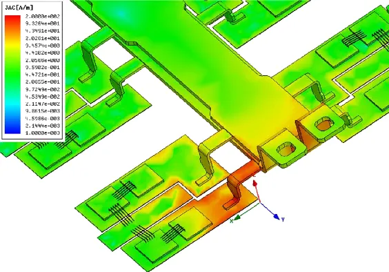
EMI reduction PCB stems from the Faraday cage-like enclosure formed by stitched planes. Stitching bridges slots that act as slot antennas, while balancing minimizes asymmetries that radiate fields. This containment suppresses both radiated and conducted emissions, crucial for compliance in dense designs. Thermal vias within stitching arrays further dissipate power, reducing junction temperatures that amplify noise.
Best Practices for Implementation
Start with stackup planning to integrate via stitching PCB and copper balancing from the outset. Define plane partitions early, then apply stitching grids with via diameters at least 0.15 mm and spacing under 1/20th of the lowest operating wavelength to ensure continuity. Adjust copper pours iteratively, using fill percentages that mirror opposite layers, and incorporate stitching vias into balance calculations as solid copper equivalents.
For ground plane improvement PCB, prioritize stitching near high-current components and trace transitions. Employ annular rings sized per fabrication capabilities to avoid stub effects. Verify balance with area calculators in design software, targeting symmetry across the entire board, not just regions.
Impedance control PCB demands coordinated efforts: route traces over continuous stitched planes and balance to hold coupling capacitance steady. Test stackups with TDR measurements post-prototype to confirm predictions.
EMI reduction PCB benefits from dense stitching along board edges and under sensitive traces. Combine with grounded guard traces for further isolation. Always simulate before committing to production, adjusting for via fence density.
Document these in fabrication drawings, specifying via plating thickness and balance tolerances. Prototype testing for warpage per IPC-A-600K acceptability criteria validates the approach.
Troubleshooting Common Challenges
Engineers encounter via stitching failures from excessive density causing drill breakout or plating voids. Mitigate by spacing vias at least 0.5 mm edge-to-edge and consulting fabricator DFM rules. Copper balancing issues manifest as warpage exceeding 0.75% of board dimension, traced to overlooked stitching contributions; recount areas including via pads.
Impedance mismatches post-fabrication often stem from unbalanced prepregs swelling unevenly. Recalculate with actual resin content data. EMI leaks through unstitched slots require denser patterns, verified via near-field scans.
Thermal hotspots arise if stitching neglects power planes; dual stitching for power and ground resolves this. Consistent application yields reliable outcomes.
Conclusion
Via stitching PCB and copper balancing form a powerful duo, driving ground plane improvement PCB, precise impedance control PCB, and effective EMI reduction PCB. Their symbiotic integration addresses electrical, mechanical, and electromagnetic challenges holistically, elevating PCB performance in demanding applications. By following structured design practices and standards like IPC-2221B and IPC-6012E, engineers unlock reliability gains without complexity. Prioritizing this relationship early in the design cycle minimizes iterations and ensures production success. Ultimately, mastering these techniques positions designs for future-proof scalability.
FAQs
Q1: What is via stitching PCB and its role in ground plane improvement?
A1: Via stitching PCB involves arrays of vias linking ground plane segments across layers to create low-inductance paths. It improves ground plane integrity by evenly distributing return currents, reducing voltage drops and resonances. This enhances signal quality in high-speed circuits and supports thermal dissipation. Proper implementation per design standards prevents fabrication defects.
Q2: How do copper balancing benefits extend to impedance control PCB?
A2: Copper balancing benefits include uniform layer copper distribution, which stabilizes dielectric thickness and prevents warpage. This maintains consistent trace-to-plane spacing, preserving characteristic impedance. Engineers achieve reliable Zo control by matching fill percentages, avoiding shifts from thermal processes. It complements stitching for overall performance.
Q3: Why is EMI reduction PCB enhanced by combining via stitching and copper balancing?
A3: EMI reduction PCB improves as stitched planes form continuous shields, bridging slots that radiate noise. Copper balancing ensures mechanical stability, preventing gaps from distortion. Together, they minimize loop areas and field leakage, crucial for dense boards. Simulations confirm effectiveness before production.
Q4: What best practices ensure effective via stitching PCB with copper balancing?
A4: Integrate via stitching grids during stackup design, accounting for their copper contribution in balance calculations. Space vias to avoid density issues and verify warpage limits. This symbiotic approach yields superior ground plane improvement PCB and impedance control PCB. Adhere to IPC guidelines for consistency.
References
IPC-2221B — Generic Standard on Printed Board Design. IPC, 2009
IPC-6012E — Qualification and Performance Specification for Rigid Printed Boards. IPC, 2017
IPC-A-600K — Acceptability of Printed Boards. IPC, 2020


