Modulation is fundamental to radio frequency (RF) wireless communication, enabling efficient transmission of information over long distances while overcoming bandwidth, interference, and regulatory constraints. In modern systems - from 5G infrastructure and IoT networks to automotive radar and industrial wireless - modulation performance depends heavily on the supporting printed circuit board. At Aivon, we focus on manufacturing RF PCBs that deliver the signal integrity, low phase noise, and impedance precision required for reliable modulation and demodulation.
This article examines key modulation principles, methods, and advanced techniques through a PCB engineering perspective.
Why Signals Are Modulated: PCB Design Challenges in Wireless Systems
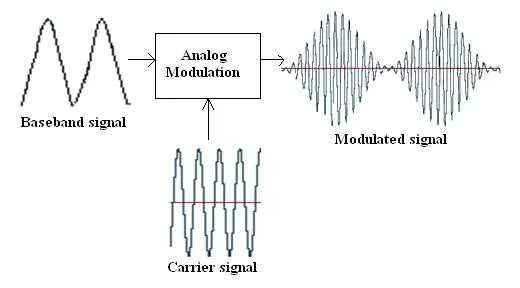
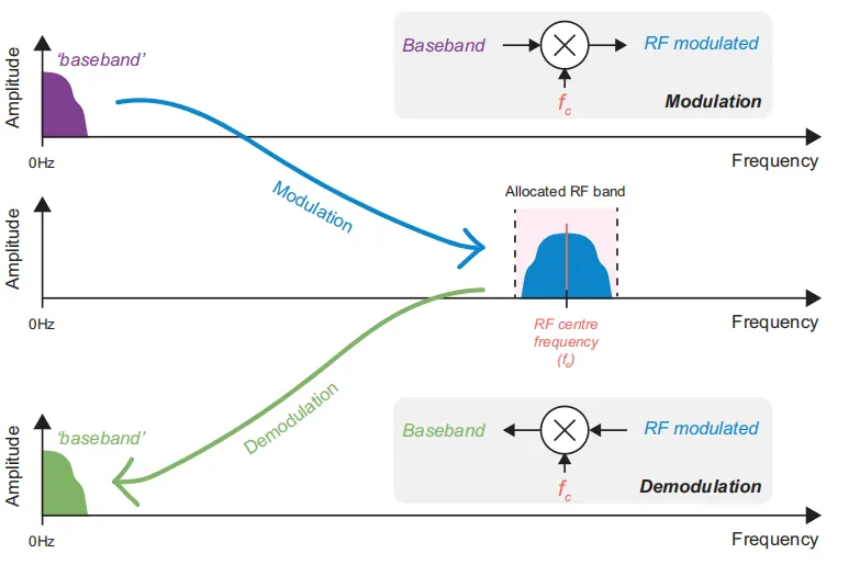
Baseband signals (voice, data, video) occupy low frequencies unsuitable for efficient radiation or long-distance propagation. Modulation shifts these signals onto higher-frequency carriers, improving antenna efficiency, spectrum utilization, and noise immunity.
Common reasons for modulation:
- Bandwidth efficiency and channel sharing
- Reduced antenna size at higher frequencies
- Improved resistance to interference and fading
- Support for multiple access techniques
PCB Implications:
High-frequency carriers demand precise transmission line design. Microstrip or coplanar waveguide traces must maintain tight impedance control (typically 50 ohms) to prevent reflections that degrade modulation accuracy. Poor layer stack-up or inconsistent dielectric thickness can introduce phase distortion and amplitude imbalance, directly impacting error vector magnitude (EVM) and bit error rates (BER).
Material selection becomes critical - low-loss laminates with stable dielectric constants help preserve signal quality across the modulation chain.
Basic and Advanced Modulation Methods for RF Systems
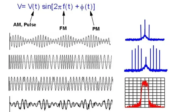
Modulation techniques fall into analog and digital categories, each presenting unique layout demands.
Analog Modulation:
- Amplitude Modulation (AM)
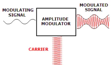
- Frequency Modulation (FM)
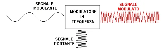
- Phase Modulation (PM)
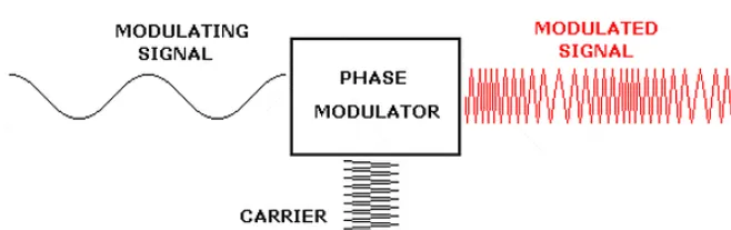
Digital Modulation (dominant in modern systems):
- Phase Shift Keying (PSK): BPSK, QPSK, 8PSK
- Quadrature Amplitude Modulation (QAM): 16QAM to 256QAM and higher
- Frequency Shift Keying (FSK) and variants like GFSK
Higher-order schemes (e.g., 64QAM+) offer greater spectral efficiency but are more sensitive to noise, phase jitter, and amplitude distortion.
PCB Design Considerations:
- Modulator circuits require excellent I/Q balance. Matched trace lengths, symmetric component placement, and differential routing minimize quadrature errors.
- High-order QAM demands superior signal integrity. Use ground plane stitching, via fencing, and shielded compartments to reduce crosstalk between digital baseband and RF sections.
- Thermal stability affects phase noise in voltage-controlled oscillators (VCOs) and phase-locked loops (PLLs). High-Tg materials and thermal vias around RFICs maintain consistent performance.
Modulation and Demodulation: Hardware Implementation on PCBs
Modulation encodes information onto a carrier, while demodulation extracts it at the receiver. Modern transceivers often integrate these functions in single RFICs, but the PCB still determines overall system performance.
Key processes include mixing, filtering, amplification, and carrier recovery. Direct conversion and superheterodyne architectures each impose different constraints.
PCB Engineering Challenges:
- Mixer and LO Paths: Local oscillator (LO) signal distribution requires low-jitter routing and isolation to prevent leakage and spurs.
- Filter Implementation: Surface acoustic wave (SAW) or ceramic filters need precise footprint design and grounding to avoid performance degradation.
- Demodulator Sensitivity: Analog front-ends are vulnerable to power supply noise. Multi-stage decoupling with LDOs near sensitive pins helps preserve carrier-to-noise ratio (CNR).
- Digital Interfaces: High-speed data lines between baseband processors and RF transceivers need length-matched, impedance-controlled routing with proper termination.
Digital Upconversion and Downconversion in RF PCBs
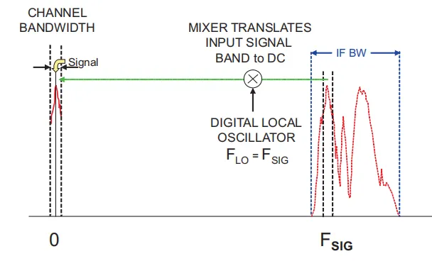
Digital Upconversion (DUC) and Digital Downconversion (DDC) use digital signal processing (DSP) to shift signals between baseband and RF frequencies. These techniques are central to software-defined radio (SDR) and multi-channel systems.
Key Operations:
- Numerically Controlled Oscillator (NCO) for frequency translation
- Digital mixing and filtering (CIC, FIR, polyphase filters)
- Interpolation and decimation for sample rate management
PCB Requirements:
- High-speed data converters (ADCs/DACs) demand excellent jitter performance on clock distribution networks. Dedicated clock layers and careful via transitions reduce phase noise.
- FPGA or DSP processors handling DUC/DDC require wide parallel buses or high-speed serial links (JESD204B/JESD204C) with rigorous length tuning and reference plane integrity.
- Power integrity is paramount during high-rate processing. Segmented power planes and localized decoupling minimize voltage ripple that could introduce spurious signals.
Spread Spectrum and Encrypted Communication Principles
Spread Spectrum techniques - Direct Sequence (DSSS), Frequency Hopping (FHSS), and Chirp Spread Spectrum - deliberately expand signal bandwidth for improved interference rejection, security, and multiple access.
These methods are foundational to GPS, Wi-Fi, Bluetooth, LoRa, and military encrypted links.
PCB Design Impact:
- Rapid frequency hopping or wideband spreading requires broadband RF paths with minimal group delay variation. Low-dispersion materials and smooth copper surfaces are essential.
- Security-focused designs often incorporate additional isolation and shielding to protect sensitive cryptographic sections from side-channel attacks.
- High processing gain in spread spectrum systems places heavy demands on digital sections, favoring high-layer count PCBs with optimized signal and power integrity.
Manufacturing Considerations:
Precision fabrication ensures consistent trace geometry and via quality, which is vital for maintaining spreading code correlation and despreading performance.
PCB Manufacturing Strategies for High-Performance RF Modulation
Successful implementation of modulation schemes requires close attention to:
- Stack-Up Design: Hybrid constructions separating RF, digital, and power domains with multiple ground planes for shielding.
- Material Selection: Rogers PCBs, Taconic PCBs, or high-performance FR4 PCBs variants with low Df and stable Dk across temperature and frequency.
- Fabrication Precision: Tight impedance tolerances, back-drilled vias, and via-in-pad technology for dense RF layouts.
- Thermal Management: Copper balancing, thermal vias, and heatsinking for power amplifiers handling modulated signals.
- Testing: VNA characterization of S-parameters, phase noise analysis, and EVM testing on finished boards.
These capabilities support demanding applications in 5G/6G base stations, autonomous vehicles, industrial IoT, medical telemetry, and consumer wireless devices.
Conclusion
From basic analog modulation to advanced digital techniques, spread spectrum, and digital conversion architectures, RF modulation places stringent requirements on PCB design and manufacturing. Signal integrity, impedance control, thermal stability, and EMI management determine whether theoretical modulation performance translates into real-world reliability.
At Aivon, our expertise in RF PCB fabrication helps engineers overcome these challenges, delivering boards optimized for today's complex wireless modulation requirements. Partnering with an experienced manufacturer ensures your modulation-based systems achieve maximum range, data rate, and robustness across diverse operating environments.