Antennas serve as the critical interface between RF circuits and free space, converting electrical signals into electromagnetic waves and vice versa. In modern wireless systems - including 5G, IoT, automotive radar, industrial sensors, and satellite communications - overall performance depends heavily on how effectively the antenna is integrated with the printed circuit board. At Aivon, we specialize in manufacturing high-frequency PCBs that optimize antenna performance through precise impedance control, material selection, stack-up design, and fabrication accuracy.
This article explores antenna principles, design considerations, radiation behavior, and integration challenges from a PCB engineering perspective.
How Antennas Work: Electromagnetic Principles and PCB Implementation
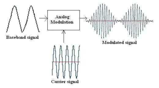
Antennas operate on the principle of reciprocity, functioning equally well for transmission and reception. When current flows through a conductor, it generates electromagnetic fields that radiate as waves. The efficiency of this process depends on resonance, impedance matching, and the physical geometry relative to the operating wavelength.
From basic parallel-wire radiators to complex array designs, antenna behavior can be analyzed through oscillator equations and wave propagation theory. Early pioneers established foundational concepts that still guide modern RF PCB layouts.
PCB Design Implications:
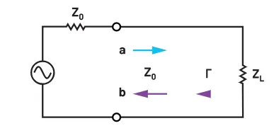
- The antenna feed point must maintain 50 ohm characteristic impedance to minimize reflections and maximize power transfer. This requires tightly controlled transmission lines (microstrip, stripline, or coplanar waveguide) with precise trace width, dielectric thickness, and copper surface roughness.
- Ground planes act as the return path and image plane. Insufficient or discontinuous ground under the antenna feed significantly degrades efficiency and radiation pattern.
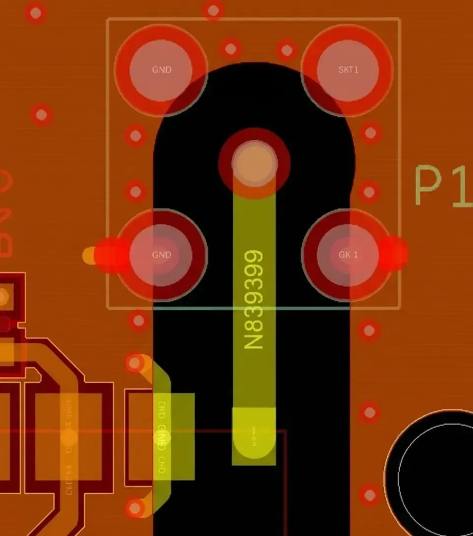
- Via transitions and connectors introduce inductance and discontinuities. Back-drilled or filled vias help maintain signal integrity at higher frequencies.
Common Antenna Types and PCB Integration Strategies
Different antenna types present unique integration challenges for PCB designers:
- Monopole and Dipole Antennas: Simple, omnidirectional designs often printed directly on the PCB or connected via coaxial feeds.
- Patch Antennas: Popular for compact, low-profile applications (GPS, Wi-Fi, 5G). Easily fabricated using copper layers on the PCB substrate.
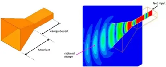
- Helical, Yagi, and Horn Antennas: External or module-based, requiring robust RF connectors and matching networks on the board.
- Array Antennas (phased arrays): Demand precise phase and amplitude control across multiple elements.
Key PCB Considerations by Type:
- Printed patch antennas require careful substrate selection (low-loss, stable dielectric constant) and exact dimensional control during etching to achieve resonance at target frequencies.
- High-gain arrays need excellent isolation between elements. Ground stitching vias and compartmentalized shielding on multilayer boards reduce mutual coupling.
- Flexible or rigid-flex PCBs enable conformal antenna designs for wearables and drones, but demand specialized lamination and material handling during manufacturing.
Antenna Radiation Patterns and Performance Factors
Radiation patterns describe how energy is distributed in space - omnidirectional, directional, or shaped. Key metrics include gain, directivity, beamwidth, front-to-back ratio, and polarization.
Earth station and satellite antennas often prioritize high gain and narrow beamwidth, while mobile and IoT devices favor broader coverage.
PCB-Related Influences on Radiation:
- Nearby components, ground plane size, and enclosure effects can distort ideal patterns. Component placement and keep-out zones are critical during layout.
- Multipath propagation - reflections from ground, walls, and objects - creates constructive and destructive interference. PCB designers mitigate this through diversity antenna schemes (spatial, polarization) with proper isolation and switching networks.
- Wave reflection at the antenna-feed interface or due to impedance mismatches leads to standing waves, reduced efficiency, and potential damage to power amplifiers.
Antenna Placement, Matching, and Environmental Considerations
Optimal antenna placement maximizes line-of-sight while minimizing interference from digital circuits, power planes, and metal structures.
Critical PCB Design Practices:
- Position antennas away from high-speed digital traces and switching regulators to preserve signal-to-noise ratio.
- Implement pi-networks or L-networks using high-Q components for fine impedance matching. Parasitic inductance from long traces or vias must be accounted for in simulation and compensated during layout.
- Thermal expansion and mechanical stress can detune antennas. High-Tg laminates and controlled coefficient of thermal expansion (CTE) materials improve stability across operating temperatures.
- For multilayer designs, dedicate specific layers for RF routing with continuous ground planes immediately adjacent to reduce EMI and provide consistent return paths.
Advanced PCB Manufacturing for Reliable Antenna Performance
Successful antenna integration requires advanced fabrication capabilities:
- Material Selection: Low-loss dielectrics (Rogers, Taconic, or premium FR4) with tight dielectric constant tolerance and low dissipation factor for minimal insertion loss and stable resonance.
- Stack-Up Optimization: Balanced constructions with dedicated RF layers, multiple ground planes, and hybrid rigid-flex options where needed.
- Fabrication Precision: Accurate etching for patch dimensions, controlled copper thickness, smooth foil profiles, and tight impedance tolerances (plus or minus 5% or better).
- Via Technology: Laser-drilled microvias, via-in-pad, and filled/stacked vias for dense, high-frequency transitions.
- Surface Finish: ENIG or ENEPIG for excellent solderability and long-term RF performance at connectors and feed points.
- Testing: Vector Network Analyzer (VNA) measurements for return loss, radiation pattern chambers, and active testing to validate real-world performance.
These techniques support demanding applications across automotive radar, 5G base stations and handsets, industrial wireless sensors, medical devices, and consumer electronics.
Conclusion
From fundamental radiation principles to complex multipath environments and high-order antenna arrays, successful RF system performance ultimately depends on expert PCB design and manufacturing. Impedance control, material stability, ground integrity, and precise fabrication determine whether an antenna delivers its theoretical gain, efficiency, and pattern in production.
At Aivon, we combine deep RF engineering expertise with state-of-the-art manufacturing to help customers achieve reliable antenna integration across diverse wireless applications. Partnering early with an experienced PCB manufacturer ensures your antenna designs meet stringent performance, reliability, and cost targets from prototype through volume production.