Introduction
In high-frequency PCB design, maintaining signal integrity stands as a critical challenge for engineers working on applications like telecommunications, radar systems, and high-speed data processing. Signals operating above several gigahertz face significant degradation from various loss mechanisms, where copper cladding plays a pivotal role in either amplifying or mitigating these issues. Copper cladding, the copper foil layers bonded to the PCB substrate, directly influences conductor losses and interactions with the dielectric material. Poor choices in cladding properties can lead to increased signal attenuation, distorting waveforms and reducing system performance. Engineers must understand how copper surface characteristics interact with electromagnetic phenomena to optimize designs. This article explores the technical principles behind copper cladding's impact on signal integrity and provides practical strategies for high-frequency PCB design.
Understanding Copper Cladding in PCBs
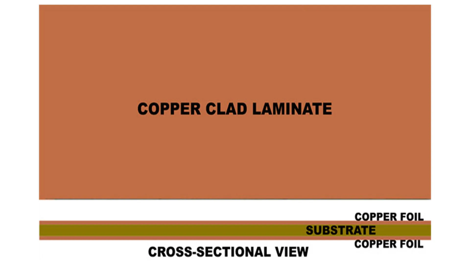
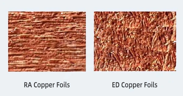
Copper cladding refers to the thin sheets of copper foil laminated onto both sides of a dielectric core material during PCB fabrication. These foils serve as the conductive pathways for signals and power distribution. In standard processes, the copper is bonded using heat and pressure, with the foil's surface treatment ensuring adhesion to the resin system. Different manufacturing methods produce variations in foil structure, such as electrodeposited foils formed through electroplating or rolled annealed foils created by mechanical rolling. Each type exhibits unique surface profiles that become increasingly relevant at higher frequencies. For high-frequency PCB design, selecting the appropriate cladding type directly affects overall board reliability and performance.
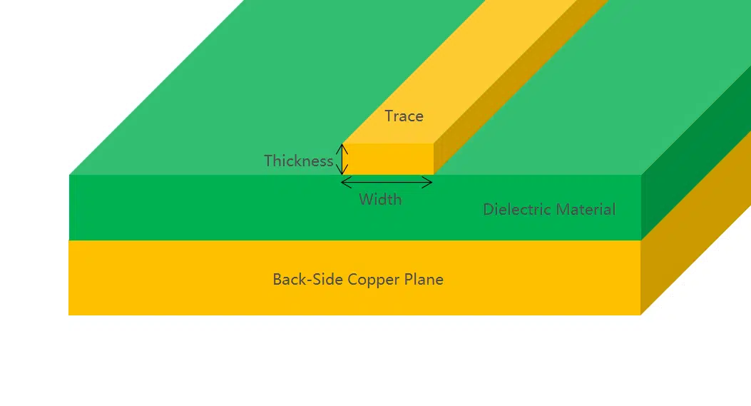
The relevance of copper cladding intensifies in high-frequency environments because signals propagate as electromagnetic waves along traces. Traditional rough surfaces, beneficial for adhesion in low-speed boards, introduce complications at gigahertz levels. Engineers evaluate cladding based on weight, typically expressed in ounces per square foot, and surface roughness parameters. These factors determine how effectively the copper conducts high-speed signals without excessive loss. Proper cladding selection aligns with industry requirements for controlled impedance and minimal distortion. Ultimately, copper cladding forms the foundation for robust signal paths in demanding applications.
Key Technical Principles: Skin Effect and Copper Cladding
The skin effect represents a fundamental phenomenon in high-frequency PCB design, where alternating current tends to concentrate near the surface of the conductor rather than distributing uniformly across its cross-section. As frequency increases, the effective conducting thickness, known as skin depth, diminishes, forcing current to flow primarily on the copper cladding's outer layer. Rough surfaces on the cladding exacerbate this by lengthening the current path, elevating resistance and contributing to conductor losses. In skin effect copper cladding scenarios, profiles with high peak-to-valley roughness amplify attenuation, particularly beyond 1 GHz. Engineers model this interaction using transmission line theory to predict signal behavior. Understanding these dynamics allows for proactive mitigation during the design phase.
Copper surface roughness directly ties into skin effect copper cladding losses, as the irregular topography increases the effective surface area exposed to the current. Standard electrodeposited foils often feature a matte side with dendritic growth, promoting adhesion but hindering high-frequency performance. Smoother alternatives reduce the magnification of resistance due to skin effect. Simulations reveal that roughness parameters like Rz or Ra correlate strongly with insertion loss measurements. Fabricators control these through specialized treatments during lamination. This principle underscores why cladding choice remains non-negotiable for preserving waveform fidelity.
Copper Cladding and Dielectric Loss Interactions
Copper cladding dielectric loss arises from the electromagnetic coupling between the conductor surface and the adjacent substrate material. At high frequencies, fields fringe into the dielectric, where surface roughness on the cladding traps energy and enhances loss tangent effects. This interaction elevates overall signal attenuation copper cladding contributes to, as the rough interface distorts field distribution. Low-profile foils minimize this by providing a flatter boundary, allowing cleaner field propagation. Engineers consider stackup configurations to separate signal layers from rough power planes. Balancing adhesion needs with loss reduction requires precise material pairing.
Dielectric polarization losses compound with cladding-induced effects, forming a composite attenuation profile. High-frequency signals experience greater sensitivity to these combined mechanisms, limiting trace lengths and data rates. Cladding treatments that smooth the copper-dielectric interface prove effective in reducing this coupling. Test structures like microstrip lines quantify the impact through S-parameter analysis. Adhering to specifications in IPC-4562 for foil profiles ensures consistency across production runs. These principles guide engineers toward designs that sustain signal quality over extended distances.
Signal Attenuation Mechanisms Linked to Copper Cladding
Signal attenuation copper cladding influences stems primarily from ohmic losses within the conductor and radiative components at discontinuities. In high-frequency PCB design, the dominant contributor at elevated frequencies shifts to surface-related conductor loss due to skin effect. Rough cladding increases the ratio of actual current path length to nominal trace width, directly boosting attenuation constants. Dielectric contributions add multiplicatively, but cladding optimization disproportionately benefits conductor-limited regimes. Engineers employ vector network analyzers to characterize these losses empirically. Mitigating attenuation demands a holistic view of cladding properties from early layout stages.
Beyond pure conductor loss, cladding imperfections induce mode conversion and crosstalk in multilayer boards. Uneven copper distribution alters characteristic impedance, exacerbating reflections. Low-roughness foils maintain uniform field confinement, preserving differential signaling integrity. IPC-2221 provides guidelines for conductor spacing and width to counteract these effects. Practical measurements confirm that smoother cladding yields lower insertion loss across broad bandwidths. Addressing signal attenuation copper cladding holistically elevates overall system margins.
Best Practices for Copper Cladding in High-Frequency PCB Design
Selecting low-profile copper foils, such as very low profile or high-performance variants, forms the cornerstone of optimizing high-frequency PCB design. These foils feature reduced surface roughness, directly countering skin effect copper cladding penalties while maintaining lamination adhesion. Engineers specify foil types early, coordinating with fabricators to match substrate compatibility. Thinner base weights suffice for signal layers, reserving heavier foils for power distribution. Stackups position low-roughness layers adjacent to sensitive dielectrics. This approach minimizes copper cladding dielectric loss without compromising mechanical integrity.
Trace geometry adjustments complement cladding choices, with wider traces compensating for increased effective resistance from skin effect. Controlled depth routing and via treatments further reduce discontinuities. Simulations incorporating foil roughness models predict attenuation accurately. IPC-6012E outlines qualification criteria for boards with performance demands, ensuring reliability. Post-fabrication verification through time-domain reflectometry validates designs. Implementing these practices systematically enhances signal margins.
Layer sequencing prioritizes signal integrity by isolating high-speed nets between ground planes with optimized cladding. Differential pairs benefit from symmetric roughness on opposing layers. Fabricators apply reverse-treat foils to promote resin flow during pressing. Environmental factors like thermal cycling test cladding adhesion per industry benchmarks. Engineers iterate stackups using field solvers for impedance control. These best practices yield robust high-frequency PCB design outcomes.
Common Challenges and Engineering Insights
Engineers often encounter unexpected attenuation spikes traceable to cladding inconsistencies across production lots. Variations in foil treatment lead to batch-dependent losses, necessitating supplier qualification. Troubleshooting involves isolating conductor versus dielectric contributions via de-embedding techniques. Common pitfalls include overlooking matte-side orientation during lamination, which orients rough surfaces toward signals. Proactive design reviews incorporate roughness specifications. Insights from field failures highlight the value of early prototyping with target foils.
Hybrid stackups blending foil types address mixed-signal requirements, using smooth cladding for RF sections. Aging effects on copper surfaces warrant accelerated life testing. Collaborative design-fabrication loops refine processes. These insights empower engineers to anticipate and resolve copper cladding-related issues efficiently.
Conclusion
Copper cladding profoundly shapes signal integrity in high-frequency PCB design by modulating skin effect, dielectric interactions, and overall attenuation. Strategic selection of low-roughness foils, informed trace geometries, and adherence to standards like IPC-4562 and IPC-2221 minimize losses effectively. Engineers achieve superior performance through integrated consideration of cladding properties from concept to verification. Practical implementation elevates designs from functional to exceptional. Prioritizing these elements ensures reliable operation in demanding high-speed environments. Future advancements in foil technology promise even greater optimizations.
FAQs
Q1: How does skin effect copper cladding impact high-frequency PCB design?
A1: Skin effect confines current to the copper surface, where cladding roughness lengthens the path and raises resistance. This elevates conductor losses, limiting signal propagation distances. Low-profile foils reduce this effect by smoothing the interface. Engineers widen traces or use simulations to compensate. Overall, optimizing skin effect copper cladding preserves bandwidth and eye diagram quality.
Q2: What role does copper cladding play in dielectric loss for PCBs?
A2: Copper cladding dielectric loss occurs as rough surfaces distort fields into the substrate, amplifying polarization losses. Smoother foils confine fields better, decoupling conductor-dielectric interactions. Stackup design positions optimal cladding near low-loss dielectrics. Measurements confirm reduced total attenuation. This focus enhances high-frequency PCB design efficiency.
Q3: How can signal attenuation copper cladding be minimized?
A3: Signal attenuation copper cladding minimizes through low-roughness foils and precise trace routing. Avoid high-peak profiles that exacerbate skin effect. Pair with low-loss substrates for synergy. Verify via S-parameters. These steps sustain signal integrity in high-frequency PCB design.
Q4: Why is copper foil selection critical in high-frequency applications?
A4: Copper foil profiles dictate conductor loss dominance at gigahertz frequencies. Standards like IPC-4562 classify options for performance matching. Low-profile types counter skin effect penalties. Engineers balance adhesion and loss for reliable boards. Proper selection drives superior high-frequency PCB design outcomes.
References
IPC-4562 — Metal Foil for Printed Wiring Applications. IPC, 2018
IPC-2221B — Generic Standard on Printed Board Design. IPC, 2012
IPC-6012E — Qualification and Performance Specification for Rigid Printed Boards. IPC, 2017


