Introduction
In the drive toward smaller, more efficient electronic devices, thin PCB technology emerges as a critical enabler. Electrical engineers increasingly face demands for compact designs in sectors like wearables, medical devices, and IoT systems. Thin PCBs allow for higher component density while maintaining electrical integrity. This guide explores thin PCB design guide principles, manufacturing processes, material choices, advantages, and applications, particularly in wearable technology. By understanding these elements, engineers can optimize performance and reliability in space-constrained projects. Factory-driven insights reveal how adherence to standards ensures production scalability.
What Are Thin PCBs and Why Do They Matter?
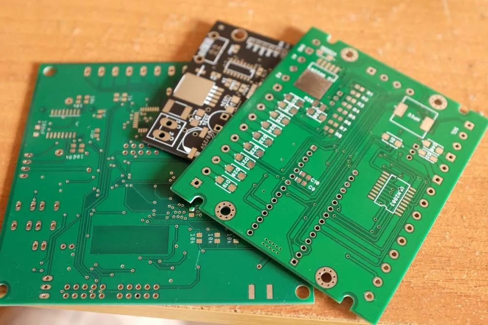
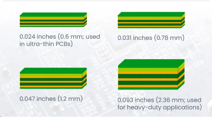
Thin PCBs refer to printed circuit boards with total thicknesses significantly below the industry standard of 1.6 mm, often ranging from 0.2 mm to 0.8 mm. This reduction in profile supports miniaturization without sacrificing functionality. Standard PCBs at 1.6 mm suit general applications, but thin variants excel where volume constraints dominate. Their relevance stems from the exponential growth in portable electronics, where every millimeter counts for user comfort and device ergonomics. Engineers must consider thin PCBs for projects requiring low profiles, as they integrate seamlessly into curved or flexible assemblies. Ultimately, thin PCB technology aligns with the shift toward high-density interconnects in modern systems.
The matter intensifies in high-volume production, where thin boards reduce material use and shipping weights. Design teams benefit from shorter signal paths, improving speed and reducing power loss. However, thinness introduces mechanical challenges that demand precise engineering. Industry trends show thin PCBs comprising a growing share of new designs, driven by consumer demand for sleeker gadgets. Electrical engineers appreciate how these boards enable innovative form factors while upholding signal integrity.
Advantages of Thin PCBs
Thin PCBs offer several key advantages that make them indispensable for miniaturization efforts. First, they enable substantial space savings, allowing more components in a smaller footprint. This density supports complex circuits in limited areas. Second, weight reduction becomes evident, critical for battery-powered devices where every gram impacts runtime. Lighter boards also ease integration into mobile systems.
Improved thermal management ranks high among benefits. Thinner dielectrics shorten heat dissipation paths from components to ambient air. This lowers junction temperatures during operation. Electrical performance enhances too, with reduced inductance in traces and better interplane capacitance for decoupling. Signal integrity improves, minimizing crosstalk in high-speed designs.
Manufacturing efficiency gains emerge from less material consumption, potentially lowering costs in high volumes. Handling thin boards requires care, but advantages outweigh for suitable applications. Flexibility increases in some materials, aiding conformal mounting. Overall, advantages of thin PCBs position them as a cornerstone for next-generation electronics.
Thin PCB Materials
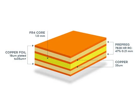
Selecting appropriate thin PCB materials ensures mechanical stability and electrical reliability. Common choices include flame-retardant epoxy resins like FR4 in ultra-thin cores, valued for cost-effectiveness and process compatibility. High glass transition temperature variants handle reflow stresses better. For demanding environments, polyimide substrates provide superior thermal resistance and flexibility.
Dielectric thickness controls directly impact impedance and capacitance. Thinner cores demand materials with low coefficient of thermal expansion to mitigate warpage. Ceramic-filled polymers suit high-frequency needs, offering low loss tangents. Copper foil weight typically drops to 1 oz/ft2 or less to maintain profile.
Material qualification follows established guidelines for consistency. Engineers balance cost, performance, and availability during selection. Thin PCB materials must exhibit uniform resin flow during lamination. Testing verifies peel strength and solderability post-processing.
Thin PCB Design Guide
A structured thin PCB design guide starts with stackup planning to control impedance and warpage. Engineers define layer count and dielectric thicknesses early, simulating thermal expansion mismatches. IPC-2221 provides generic requirements for board design, including spacing rules adjusted for thin profiles. Trace widths widen slightly to compensate for reduced rigidity, preventing fractures.
Component placement prioritizes balance to minimize bow and twist. Support vias or fiducials aid assembly fixturing. Signal routing favors shorter paths, incorporating ground planes for shielding. Power distribution networks require careful decoupling placement due to proximity effects.
Design for manufacturability includes panelization on carriers for thin singles. Solder mask and silkscreen thicknesses scale down proportionally. Finite element analysis predicts warpage under load. Validation through prototypes confirms electrical margins. This logical approach yields robust thin PCB designs.
Thin PCB Manufacturing Process
The thin PCB manufacturing process mirrors standard flows but incorporates specialized handling to combat fragility. It begins with thin core preparation, where copper-clad laminates undergo precise cutting. Inner layers pattern via photolithography and etching, followed by black oxide treatment for adhesion. Lamination presses thin prepregs under controlled pressure and temperature to form multilayers.
Drilling employs laser for microvias, as mechanical bits risk breakout on thin stock. Desmear removes residue, enabling electroless copper deposition. Plating builds up traces, with pattern electroplating for definition. Outer layers image, etch, and apply solder mask. IPC-6012 outlines qualification specs for rigid boards, ensuring performance metrics like conductor width tolerance.
Final steps include electrical testing, routing from carrier panels, and inspection per IPC-A-600 criteria for acceptability. Baking controls moisture prior to shipping. Process controls emphasize cleanliness to avoid defects amplified by thinness. Yield optimization relies on statistical process control.
Thin PCB Applications in Wearable Technology
Thin PCB applications in wearable technology thrive due to form factor demands. Fitness trackers integrate thin boards for slim profiles, housing sensors and batteries comfortably. Smartwatches leverage them for curved enclosures, enabling vibrant displays alongside processing. Medical patches use flexible thin variants for skin conformance, monitoring vitals continuously.
In hearing aids, ultra-thin rigid-flex hybrids deliver audio processing in ear canals. AR glasses employ thin PCBs for lightweight optics control. These applications demand biocompatibility and low power. Thinness facilitates bending radius compliance in dynamic wear.
Assembly challenges include fine-pitch components, addressed via advanced stencils. Reliability testing simulates daily motions. Thin PCB applications in wearable technology drive innovation in health and fitness sectors.
Challenges and Best Practices
Thin PCBs present challenges like warpage from asymmetric copper distribution and handling damage. Best practices include symmetric stackups and carrier frames during fabrication. Engineers specify bow and twist limits upfront, typically under 0.75% for class 2 assemblies.
Assembly requires vacuum fixturing to prevent flexing under pick-and-place. Reflow profiles adjust for thinner mass, reducing ramp rates. Strain gauging during prototyping identifies weak points. Material selection prioritizes low CTE for stability.
Quality control verifies via automated optical inspection tailored for thin features. Documentation details handling protocols. These practices ensure high yields and field reliability.
Conclusion
Thin PCB technology unlocks miniaturization across demanding applications. Key advantages include space efficiency, thermal benefits, and electrical gains. Proper materials, design per IPC guidelines, and refined manufacturing processes mitigate risks. Applications in wearables exemplify their transformative potential. Electrical engineers equipped with this knowledge can deliver superior designs. Future advancements will further refine thin PCB capabilities.
FAQs
Q1: What is a thin PCB design guide essential for?
A1: A thin PCB design guide ensures impedance control, warpage minimization, and assembly compatibility in compact systems. Engineers follow structured stackups and spacing rules from IPC-2221 to balance density and reliability. This approach prevents common pitfalls like signal distortion. Practical simulations validate choices early.
Q2: How does the thin PCB manufacturing process differ from standard boards?
A2: The thin PCB manufacturing process uses laser drilling, carrier panelization, and precise lamination to handle fragility. Controls focus on warpage and cleanliness, aligning with IPC-6012 specs. Steps like plating and testing scale for thin profiles. This yields high-quality boards for miniaturization.
Q3: What are the main advantages of thin PCBs in high-density designs?
A3: Advantages of thin PCBs include reduced weight, better heat dissipation, and enhanced signal integrity through shorter paths. They enable higher component packing without bulk. Electrical engineers gain from lower inductance in wearables. Trade-offs like strength require careful design.
Q4: Where do thin PCB applications in wearable technology shine?
A4: Thin PCB applications in wearable technology excel in smartwatches, sensors, and patches needing slim, flexible forms. They support conformal mounting and battery life extension. Reliability under motion demands robust materials. Integration drives user comfort and functionality.
References
IPC-2221B — Generic Standard on Printed Board Design. IPC, 2003
IPC-6012E — Qualification and Performance Specification for Rigid Printed Boards. IPC, 2017
IPC-A-600K — Acceptability of Printed Boards. IPC, 2020


