Introduction
In modern electronics, PCB panel size impedance becomes a critical factor when designing controlled impedance PCB panels for high-speed applications. Engineers must balance manufacturing efficiency with the need to preserve PCB panel signal integrity across transmission lines. Larger panels allow for higher production yields by accommodating multiple boards, but they introduce variations in material properties and process tolerances that can compromise impedance consistency. This is particularly vital in PCB panel high-speed design, where even minor deviations lead to signal reflections, crosstalk, and data errors. Understanding these interactions ensures reliable performance in devices operating at gigabit speeds. Proper design considerations mitigate risks while optimizing costs.
Fundamentals of PCB Panelization and Impedance Control
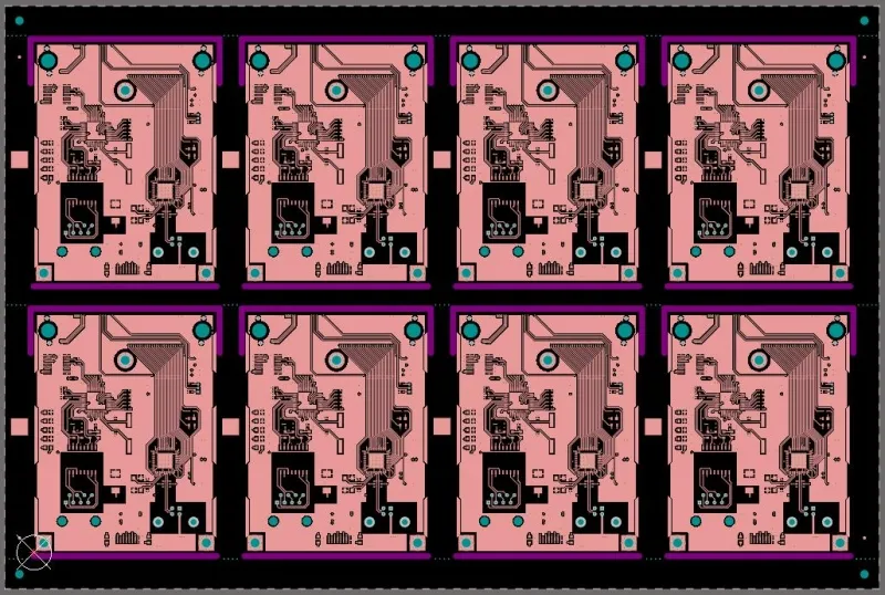
PCB panelization involves arranging multiple individual boards on a single substrate panel to streamline fabrication and assembly processes. Standard panel dimensions influence how uniformly manufacturing steps like lamination, etching, and plating occur across the array. In controlled impedance PCB panel production, impedance refers to the characteristic impedance of traces, typically targeted at 50 ohms or 100 ohms differential for PCB panel transmission lines. Variations arise from dielectric thickness inconsistencies, copper weight differences, and thermal expansion mismatches amplified by panel expanse. Engineers evaluate these effects early to specify panel configurations that maintain tight tolerances. Adhering to IPC-2221 guidelines helps establish baseline design rules for such layouts.
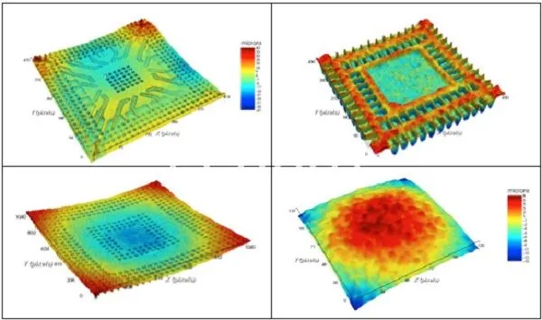
Panel size directly impacts warpage, a common issue where the board bows due to asymmetric copper distribution or resin shrinkage during curing. Larger panels exacerbate this because stresses accumulate over greater areas, altering the effective dielectric height between traces and reference planes. This shifts impedance values, potentially exceeding acceptable limits for high-speed signals. Manufacturers often recommend limiting panel size based on board thickness and layer count to minimize these distortions. Fiducial marks and tooling holes must be strategically placed to ensure alignment precision across the panel. By simulating these factors, designers predict and counteract potential deviations.
Technical Principles of Impedance in PCB Panels
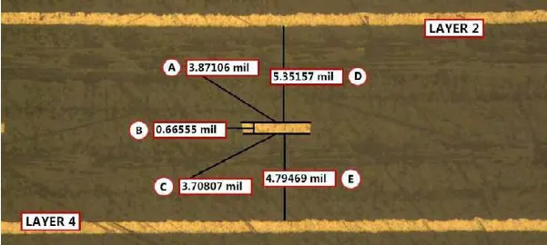
Impedance in PCB panel transmission lines follows transmission line theory, where characteristic impedance Z0 depends on trace geometry and surrounding dielectrics. For microstrip lines on outer layers, Z0 is influenced by trace width, substrate height, and effective dielectric constant. Striplines embedded between planes offer better shielding but demand precise core and prepreg thicknesses. Panel size introduces spatial variations, as inner layer registration drifts farther from the center, affecting etch accuracy. These nonuniformities degrade PCB panel signal integrity, causing impedance mismatches that reflect signals back toward the source. Engineers calculate Z0 using field solver models that account for panel-scale effects.
Material properties like dielectric constant (Dk) and dissipation factor (Df) vary slightly across large panels due to resin flow during lamination. Thicker panels or those with high aspect ratios amplify copper plating thickness gradients from panel edges to center. Such gradients alter trace resistance and capacitance per unit length, directly impacting Z0. IPC-2141 provides detailed methods for modeling these controlled impedance scenarios in high-speed logic designs. Temperature and humidity during processing further modulate Dk, emphasizing the need for controlled environments. Comprehensive stackup documentation, including panel layout, is essential for repeatability.
Design Considerations for Optimal Panel Size
Selecting PCB panel size requires evaluating trade-offs between throughput and precision for PCB panel high-speed design. Smaller panels reduce warpage and process variations, enabling tighter impedance tolerances like plus or minus 5 percent. However, they increase handling costs and setup times per batch. Larger panels boost economy for volume production but demand enhanced fixturing and stress-relief features like breakaway tabs. Board outline complexity and depanelization method, such as routing or scoring, influence feasible sizes. Simulations of thermal-mechanical behavior predict bow and twist limits per IPC-6012 performance specifications.
Trace routing strategies must adapt to panel dimensions to preserve signal integrity. High-speed nets benefit from centering critical transmission lines away from edges, where material thinning occurs during routing. Reference plane splits should avoid running parallel to panel boundaries to prevent return path discontinuities. Via farms or dense pin fields at panel peripheries can induce localized heating, skewing nearby impedances. Designers incorporate impedance test coupons at multiple panel locations, such as corners and center, to verify uniformity. This data informs adjustments before full production.
Aspect ratio of the panel, defined as length to width, affects lamination pressure distribution. Elongated panels experience uneven squeeze-out of resin, leading to thickness gradients that alter stripline impedances. Square or near-square panels promote more uniform flow. Copper balance across layers counters asymmetric stresses, maintaining flatness. For multilayer boards, sequential lamination processes benefit from modular panel arrays that limit size per build cycle. These considerations ensure controlled impedance PCB panel reliability under operational stresses.
Best Practices for Impedance Control Across Panels
Implement a robust stackup with symmetric builds to minimize warpage in PCB panel size impedance management. Specify core and prepreg thicknesses with tight tolerances, verified through cross-section analysis. Use field solvers calibrated to actual material datasheets for initial Z0 predictions, then refine with TDR measurements on fabricated coupons. Place at least four impedance test structures per panel, positioned to capture edge and center variations. Route high-speed pairs with length matching and constant spacing to uphold differential impedance. Avoid right-angle bends in transmission lines, opting for smooth curves to reduce reflections.
Material selection plays a pivotal role; low-loss dielectrics with stable Dk suit PCB panel transmission lines in high-speed designs. Hybrid stacks combining FR-4 with higher-frequency cores control costs while meeting performance. Etch compensation factors must scale with panel size to achieve nominal trace widths. Post-etch inspection via automated optical systems confirms dimensional accuracy. For assemblies, ensure depanelization does not introduce microcracks that propagate stress. These practices align with IPC-2141 recommendations for high-speed controlled impedance.
Verification extends beyond coupons; full-panel TDR or VNA sweeps map impedance profiles. Thresholds for acceptability depend on bit error rates tolerated in the application. Feedback loops with fabricators refine panel designs iteratively. Software tools model panel effects by incorporating manufacturing tolerances as statistical distributions. Ground plane stitching vias near high-speed transitions stabilize reference potentials. Comprehensive documentation transfers knowledge for scaled production.
Signal Integrity Optimization in Large Panels
Large PCB panels challenge PCB panel signal integrity due to accumulated tolerances in multilayer alignment. Misregistration shifts trace-to-plane spacing, elevating loop inductance and crosstalk. Engineers mitigate this by specifying tighter drill-to-copper tolerances and using blind or buried vias for dense routing. Eye diagram simulations incorporating panel variations predict jitter margins. Pre-layout analysis of power distribution networks ensures low noise injection into signals. Post-layout reviews flag potential hotspots from panel edge effects.
Crosstalk coupling strengthens over longer parallel runs common in panelized arrays. Segregate aggressor and victim nets with ground shielding or increased spacing. Differential signaling benefits from tight pair geometries maintained via design rules. Thermal vias in power planes dissipate heat evenly, preventing localized Dk shifts. These strategies uphold impedance profiles under dynamic conditions.
Conclusion
Mastering PCB panel size and impedance control demands a holistic approach integrating design, materials, and manufacturing insights. By prioritizing uniformity through strategic sizing, robust stackups, and verification, engineers achieve superior PCB panel signal integrity. Adopting these considerations elevates PCB panel high-speed design reliability while optimizing yields. Continuous refinement based on test data ensures evolving performance needs are met. Ultimately, disciplined practices deliver products that perform consistently in demanding environments.
FAQs
Q1: What factors influence PCB panel size impedance in high-speed designs?
A1: PCB panel size impedance varies due to warpage, dielectric thickness gradients, and etching nonuniformities across larger areas. Smaller panels reduce these effects for tighter control, while larger ones require enhanced fixturing and balanced copper distribution. Test coupons at multiple locations verify consistency, aligning with standards like IPC-2141 for controlled impedance PCB panel applications. Proper stackup symmetry further stabilizes transmission lines.
Q2: How do you ensure controlled impedance PCB panel uniformity?
A2: Achieve controlled impedance PCB panel uniformity by distributing impedance coupons evenly and using TDR for verification. Symmetric layer builds minimize warpage impacting trace heights. Material specs with low Dk variation and precise lamination controls counteract panel-scale effects. Design rules enforce trace geometries accounting for process tolerances, preserving PCB panel transmission lines integrity.
Q3: Why is PCB panel size critical for signal integrity?
A3: PCB panel size affects PCB panel signal integrity through amplified process variations like plating thickness and registration errors on larger substrates. These cause impedance mismatches leading to reflections and eye closure in high-speed signals. Optimal sizing balances yield with precision, incorporating fiducials for alignment. IPC-2221 guidelines aid in defining layouts that sustain performance.
Q4: What best practices improve PCB panel high-speed design?
A4: For PCB panel high-speed design, center critical nets away from edges, match lengths for pairs, and shield with ground planes. Simulate panel effects on impedance using statistical models. Verify with full-panel scans post-fabrication. Balanced copper and modular arrays limit distortions, ensuring reliable transmission lines.
References
IPC-2141A — Design Guide for High-Speed Controlled Impedance Circuit Boards. IPC.
IPC-2221B — Generic Standard on Printed Board Design. IPC.
IPC-6012E — Qualification and Performance Specification for Rigid Printed Boards. IPC, 2017


