Introduction
When starting a new electronic project as a hobbyist, selecting the right printed circuit board (PCB) can make or break your build. PCB thickness plays a crucial role in determining how well your board handles mechanical stress, electrical performance, and overall reliability. A PCB thickness comparison between thick and thin options reveals trade-offs that directly impact project success, from simple LED displays to more ambitious motor controllers. Understanding these differences helps beginners avoid common pitfalls like warpage or overheating. This guide breaks down the essentials of thick PCB vs standard PCB choices, offering a PCB thickness guide for beginners to make informed decisions. By the end, you’ll know the advantages of thick PCB vs thin PCB and how to choose the right PCB thickness for your needs.
What Is PCB Thickness and Why Does It Matter?
PCB thickness refers to the overall height of the board, measured from the bottom copper layer to the top solder mask, typically influenced by the core material, copper weight, and prepreg layers. Standard thicknesses hover around common values used in hobbyist prototypes, while thick PCBs exceed these for added rigidity and thin ones dip below for compactness. This dimension affects everything from manufacturing feasibility to end-use durability in electronic projects. For instance, in a drone controller, a mismatched thickness could lead to vibration failures, whereas in a wearable gadget, it might determine fit and flexibility. Why it matters boils down to balancing mechanical strength with size constraints, ensuring your project performs reliably under real-world conditions. Hobbyists often overlook this, leading to redesigns, but a solid PCB thickness guide for beginners starts with recognizing these foundational impacts.
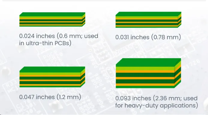
Understanding Standard PCB Thicknesses
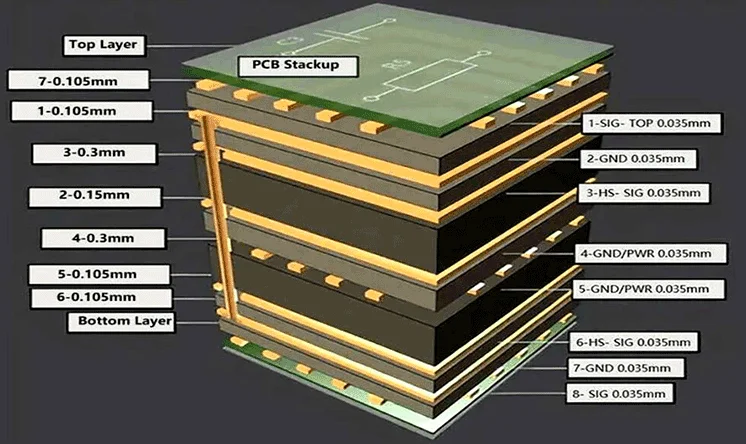
In the PCB industry, thicknesses are categorized relative to a baseline often seen in single-layer or double-layer boards suitable for hobbyist work. Standard PCBs generally fall into a range that supports most prototyping needs without excessive cost or complexity. Thick PCBs, on the other hand, incorporate heavier copper foils or more dielectric layers, providing robustness for power-heavy applications. Thin PCBs prioritize minimal height, ideal for stacking in tight enclosures or high-density interconnects. These variations stem from the laminate stackup, where each layer adds incrementally to the total height. Manufacturers adhere to tolerances outlined in standards like IPC-6012, which specifies qualification for rigid printed boards, ensuring consistency across production runs.
The choice between thick PCB vs standard PCB hinges on project demands, with hobbyists benefiting from starting with standard options for quick iterations. Deviating to thicker boards requires considering tooling adjustments during fabrication, while thinner ones demand precise handling to prevent damage.
Technical Principles Behind Thick and Thin PCBs
The core material, usually FR-4 glass epoxy, dictates baseline thickness, but copper thickness and layer count amplify it. Thicker boards distribute mechanical loads better across a larger cross-section, reducing deflection under bending forces common in handheld devices. This principle follows basic beam theory, where increased height exponentially boosts stiffness. Electrically, thicker dielectrics allow higher voltage standoff but may introduce minor impedance variations in high-speed signals. Thermally, thick PCBs offer superior heat spreading due to greater mass, aiding components like power transistors in hobby amplifiers. Thin PCBs, conversely, excel in scenarios needing low inductance paths, as shorter dielectric distances minimize parasitic effects.
Warpage becomes a key concern, especially post-soldering reflow, where asymmetric copper distribution on thin boards exacerbates bowing. IPC-A-600 provides acceptability criteria for such defects, guiding inspections in quality control. Factory processes mitigate this through symmetric stackups and controlled curing, but hobbyists can simulate risks by mocking up designs. In multilayer boards, prepreg thickness uniformity ensures the final height meets specs, preventing interlayer shorts.
Advantages of Thick PCB vs Thin PCB
Thick PCBs shine in applications requiring durability, such as automotive-inspired hobby projects or rugged enclosures. Their primary advantage lies in mechanical stability, resisting flex that could crack solder joints over time. They handle higher currents without excessive voltage drop, thanks to thicker copper options, making them suitable for motor drivers or battery chargers. Heat dissipation improves with more thermal mass, allowing passive cooling in compact builds. Cost-wise, while material use increases, the reduced failure rate offsets prototyping expenses for iterative projects.
Thin PCBs offer compelling benefits for space-constrained designs, like IoT sensors or portable gadgets. They reduce overall weight, enhancing battery life in mobile projects, and enable tighter mechanical fits. High-frequency performance benefits from lower loop inductance, ideal for RF hobby antennas. Manufacturing yields can be higher for thin boards due to simpler lamination, though handling demands care. In a PCB thickness comparison, thick options prioritize longevity, while thin ones favor agility and miniaturization.
- Mechanical: Thick — high rigidity, low warpage; Thin — lightweight, flexible integration.
- Electrical: Thick — high current capacity; Thin — low inductance for signals.
- Thermal: Thick — better heat spreading; Thin — compact cooling solutions.
- Cost/Application: Thick — durable for power applications; Thin — affordable for compact prototypes.
Choosing the Right PCB Thickness: A Beginner’s Guide
Selecting PCB thickness starts with defining your project’s environmental and functional needs. For hobbyists building LED matrices or Arduino shields, standard thickness suffices for cost-effective reliability. Assess power requirements: high-amp circuits lean toward thicker boards to minimize trace widths and heat. Mechanical mounting points, like standoffs or enclosures, influence choices, with thick PCBs providing secure fastening. Layer count correlates directly; more layers naturally increase height, so optimize routing to stay lean.
Consult design guidelines from IPC-2221 for land pattern and spacing, which indirectly tie to thickness tolerances. Simulate thermal profiles using basic spreadsheets to predict hotspots. Prototype with standard first, then iterate to thick or thin based on tests. Factor in assembly: thin boards risk bending during soldering, while thick ones need adjusted stencil apertures. This PCB thickness guide for beginners emphasizes starting simple and scaling based on validation.
Best Practices for PCB Thickness in Hobby Projects
Always specify thickness explicitly in your fabrication files, including tolerances like ±10% for standard processes. Balance copper weight symmetrically to minimize warpage, a practice aligned with IPC standards for multilayer qualification. For thick PCBs, incorporate thermal vias under power components to leverage the board’s mass effectively. Thin PCB users should reinforce edges with frame tabs during fab to ease handling. Test prototypes under vibration using simple shaker setups to validate mechanical choice.
Incorporate fiducials for precise alignment, especially on thin boards prone to shift. Document stackup details for repeatability, aiding future revisions. Collaborate with fabricators early on custom thicknesses to avoid yield issues. These steps ensure advantages of thick PCB vs thin PCB are fully realized without surprises.
Real-World Insights for Electronic Hobbyists
Consider a hobby robot chassis PCB: a thick variant withstands gear motor vibrations, preventing trace fractures seen in thinner prototypes. Conversely, a thin PCB in a smartwatch mockup allows slim profiling, though it required conformal coating for humidity protection. These examples highlight how PCB thickness comparison informs trade-offs in dynamic projects. Troubleshooting warpage? Measure bow with a straightedge and adjust copper balance. Factory insights stress pre-bake for moisture control per J-STD-020, applicable to home reflow ovens. Such practical tweaks elevate hobby builds to professional grades.
Conclusion
Decoding PCB thickness empowers hobbyists to match board specs to project realities, optimizing performance and reliability. From mechanical robustness in thick designs to compact efficiency in thin ones, each has distinct roles in your electronic endeavors. Use this PCB thickness guide for beginners to weigh factors like power, size, and durability systematically. Prioritize standards-compliant practices for consistent results, avoiding costly redesigns. Ultimately, choosing the right PCB thickness transforms prototypes into enduring creations, fueling your next innovation.
FAQs
Q1: What is a standard PCB thickness for beginner projects?
A1: Standard PCB thickness, often around hobbyist baselines, suits most simple circuits like sensors or displays. It balances cost, strength, and ease of soldering without specialized tools. For a PCB thickness comparison, stick to this unless power or rigidity demands thick PCB vs standard PCB adjustments. Always check tolerances to ensure fit in enclosures.
Q2: What are the main advantages of thick PCB vs thin PCB in electronics?
A2: Thick PCBs provide superior mechanical strength and heat handling, ideal for power supplies or motors in hobby projects. Thin PCBs save space and weight, perfect for wearables or drones. This PCB thickness guide for beginners notes thick options reduce warpage risks, while thin ones enable dense layouts. Choose based on your project’s primary stresses.
Q3: How do I choose the right PCB thickness for my project?
A3: Evaluate electrical loads, mechanical environment, and size constraints first. Standard works for prototypes; go thicker for durability or thinner for compactness. Consult IPC guidelines for tolerances in your PCB thickness comparison. Test small batches to validate, ensuring advantages of thick PCB vs thin PCB align with performance.
Q4: Can thin PCBs handle high-power hobby applications?
A4: Thin PCBs manage moderate power with careful trace design but falter under sustained high currents compared to thick options. Enhance with heatsinks or vias for better dissipation. In choosing right PCB thickness, prioritize thick for amps above a few, per standard practices, to avoid overheating in projects like amplifiers.
References
IPC-6012E — Qualification and Performance Specification for Rigid Printed Boards. IPC, 2017
IPC-A-600K — Acceptability of Printed Boards. IPC, 2020
IPC-2221B — Generic Standard on Printed Board Design. IPC, 2012
J-STD-020E — Moisture/Reflow Sensitivity Classification for Nonhermetic Surface Mount Devices. JEDEC, 2014


