Introduction
PCB outlines form the foundational boundary of any printed circuit board, dictating its physical form and influencing every stage from design to deployment. For electrical engineers, mastering PCB outline creation ensures seamless integration with enclosures, reliable mechanical performance, and optimal manufacturability. Poorly defined outlines can lead to assembly challenges, stress concentrations, and fabrication defects that compromise board reliability. This guide delves into PCB outline design rules, validation techniques, and manufacturability considerations, providing structured insights for robust designs. By adhering to established principles, engineers can minimize risks and enhance product longevity. Understanding these elements empowers precise PCB outline creation tailored to demanding applications.
What Is a PCB Outline and Why It Matters
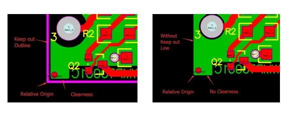
A PCB outline defines the external perimeter and internal cutouts of the board, specified on a dedicated mechanical layer in design files. It encompasses the board's overall shape, edge finishes, mounting holes, and fiducials for alignment during fabrication and assembly. This outline serves as the blueprint for routing, scoring, or milling processes that shape the final product. In electrical engineering contexts, the PCB outline directly impacts mechanical stability, thermal dissipation paths, and electrical isolation from edges.
The significance of precise PCB outline design rules cannot be overstated, as they prevent issues like board warpage, cracking under thermal cycling, or misalignment in automated assembly. For instance, outlines that ignore material expansion coefficients risk dimensional instability in multilayer boards. Manufacturability hinges on outlines that accommodate standard tooling and processes, reducing scrap rates and costs. Engineers must prioritize outlines that balance functionality with fabrication feasibility from the outset. Neglecting these aspects often results in iterative redesigns, delaying time-to-market.
Technical Principles of PCB Outline Creation
PCB outline creation begins with defining the board's geometry based on system requirements, such as enclosure fit and component placement constraints. Engineers sketch the perimeter using straight lines, arcs, and splines, ensuring all features align with the board's stackup and layer count. Internal cutouts for connectors or heat sinks require careful positioning to maintain structural integrity. The outline must incorporate tooling features like fiducial marks and registration holes, typically placed symmetrically for precision machining.
Key PCB outline design rules govern edge treatments to mitigate stress risers. Sharp corners invite microcracks during depanelization or handling, so fillets with adequate radii prove essential. Clearances between traces, components, and the outline prevent electrical shorts and mechanical interference. According to IPC-2221, generic design guidelines emphasize minimum edge-to-copper distances to safeguard against etching undercuts and routing inaccuracies. These principles extend to multilayer boards, where via staggering near edges avoids drill breakout.
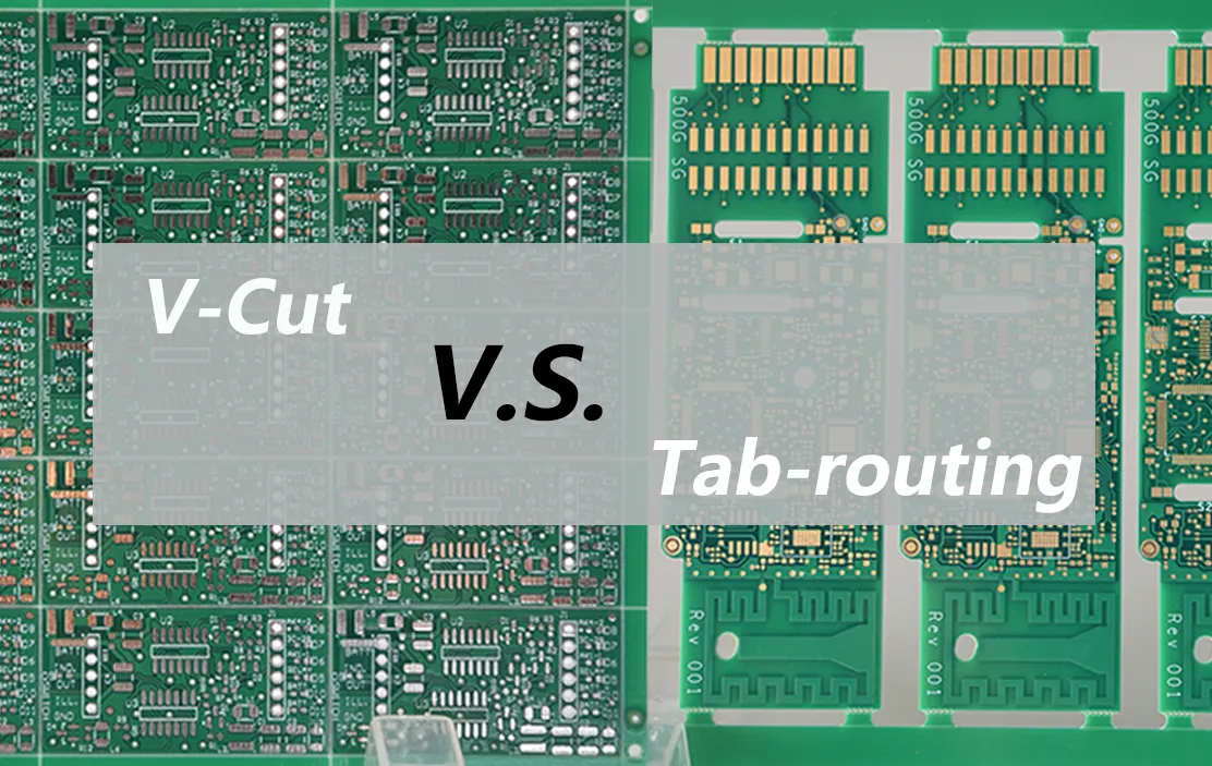
Panelization integrates multiple outlines into a production panel, optimizing throughput for volume manufacturing. V-scoring suits straight-edged rectangular boards, while tab routing handles complex shapes. Each method imposes rules on spacing between individual outlines and panel borders to facilitate clean separation. Engineers evaluate panel efficiency by considering fiducial placement and breakaway tabs that minimize burrs.
PCB Outline Design Rules for Optimal Performance
Adhering to PCB outline design rules starts with dimensional stability considerations tied to laminate properties and thickness. Thinner boards demand tighter rules to counter flexure, while thicker ones tolerate larger features. Minimum internal radii for cutouts and slots prevent tool breakage and ensure smooth milling paths. Horizontal and vertical scoring lines require uniform widths across the panel to maintain parallelism.
Edge clearance rules specify distances from the outline to high-voltage traces or sensitive components, reducing arcing risks. Mounting holes positioned near corners distribute loads evenly, countering torque from connectors. IPC-6012 outlines qualification criteria for rigid boards, including dimensional accuracy post-fabrication. Compliance with these rules enhances yield by aligning designs with process capabilities.
For high-density interconnects, outline rules incorporate beveling or chamfering to ease insertion into housings. Symmetrical shapes minimize warpage from asymmetric copper distribution. Engineers apply these rules iteratively, simulating mechanical stresses to refine geometries.
Practical Solutions and Best Practices for PCB Outline Validation
PCB outline validation involves systematic checks against design rules and manufacturability criteria early in the workflow. Design rule checks (DRC) flag violations like insufficient radii or overlapping features. Finite element analysis (FEA) models outline stresses under thermal loads, predicting potential failures. Visual inspections verify layer alignment, especially for stepped outlines in rigid-flex boards.
To ensure PCB outline manufacturability, collaborate with fabrication parameters such as routing bit diameters and scoring depths. Specify outline tolerances that reflect process capabilities, avoiding overly tight specs that inflate costs. Dry runs with prototype panels reveal depanelization issues like tab fractures. Post-fabrication metrology confirms outline fidelity using coordinate measuring machines.
Best practices include standardizing fiducial patterns for optical alignment and incorporating breakaway rails for handling. For V-scored panels, maintain consistent groove depths to prevent partial cuts. Tab-routed designs benefit from perforated mouse bites that shear cleanly without stressing components.
Troubleshooting Common PCB Outline Issues
Electrical engineers frequently encounter outline-related challenges that manifest during prototyping or production. Warpage arises from unbalanced copper or improper panelization, distorting fiducials and assembly accuracy. Stress cracks at corners stem from acute angles or inadequate radii, exacerbated by thermal mismatch. Validation reveals these via shadow moiré interferometry or dial gauge measurements.
Misaligned outlines result from artwork scaling errors or asymmetric drill patterns. Troubleshooting involves reviewing stackup symmetry and adjusting copper pours. Depanelization defects, such as burrs from dull tools, trace back to outline complexity exceeding machine limits. Iterative validation refines designs, incorporating lessons into templates.
Complex shapes demand hybrid panelization, combining scoring and routing for manufacturability. Engineers document root causes in design reviews to prevent recurrence.
Conclusion
Mastering PCB outlines requires a holistic approach encompassing creation, design rules, validation, and manufacturability. Electrical engineers who integrate these elements from concept to fabrication achieve boards that excel in reliability and performance. Structured adherence to principles like edge clearances and panelization optimizes outcomes. Proactive validation mitigates risks, ensuring designs translate smoothly to production. By prioritizing these practices, teams reduce iterations and elevate quality. This foundation equips engineers to tackle advanced applications confidently.
FAQs
Q1: What are the key steps in PCB outline creation?
A1: PCB outline creation starts with defining the perimeter based on mechanical constraints, followed by adding cutouts and tooling features. Incorporate fillets for corners and clearances for traces to align with PCB outline design rules. Validate geometry against stackup and simulate stresses. This process ensures compatibility with fabrication tools, enhancing overall manufacturability.
Q2: How do PCB outline design rules impact board reliability?
A2: PCB outline design rules dictate minimum radii, edge distances, and hole placements to prevent stress concentrations and electrical issues. They promote uniform load distribution and thermal stability. Adhering to standards like IPC-2221 minimizes warpage and cracking. Proper rules directly boost long-term reliability in operational environments.
Q3: What techniques improve PCB outline validation?
A3: PCB outline validation employs DRC software, FEA for mechanical analysis, and prototype inspections. Check tolerances, fiducial accuracy, and depanelization paths. Metrology tools confirm post-process dimensions. These methods catch manufacturability flaws early, avoiding costly revisions.
Q4: Why is PCB outline manufacturability critical for production?
A4: PCB outline manufacturability ensures designs suit routing, scoring, and panelization processes, reducing defects and costs. Factors like tool access and material stability influence yield. Optimized outlines with standard features streamline high-volume runs. Neglect here leads to scrap and delays.
References
IPC-2221 - Generic Standard on Printed Board Design. IPC, 2009
IPC-6012E - Qualification and Performance Specification for Rigid Printed Boards. IPC, 2017
IPC-A-600K - Acceptability of Printed Boards. IPC, 2020


