Introduction
Printed circuit boards form the backbone of modern electronics, where mechanical stability directly influences overall system performance. PCB layer thickness, encompassing copper foil and dielectric materials, plays a pivotal role in determining PCB mechanical strength and PCB reliability. Engineers must consider how variations in these thicknesses affect the board's ability to withstand physical stresses, such as vibration and component loads. In high-stakes applications like automotive or industrial controls, inadequate layer thickness can lead to warpage, fatigue cracks, or solder joint failures. This article explores the engineering principles behind layer thickness effects, offering structured insights for optimizing designs. By understanding these relationships, electrical engineers can enhance PCB vibration resistance and component weight support without compromising functionality.
Defining PCB Layer Thickness and Its Fundamentals
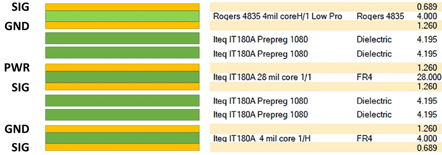
PCB layer thickness refers to the dimensions of individual layers in the stackup, primarily copper conductors measured in ounces per square foot and dielectrics like cores and prepregs in mils or micrometers. Standard copper thicknesses range from 0.5 oz to 3 oz or more, while dielectric layers vary to achieve total board thicknesses from 0.4 mm to over 3 mm. These parameters define the board's structural hierarchy in multilayer constructions. Thinner layers enable compact, high-density designs but challenge mechanical integrity. Conversely, thicker layers bolster rigidity yet increase material costs and weight. Grasping these basics allows engineers to balance electrical, thermal, and mechanical demands effectively.
Engineering Mechanisms of Layer Thickness on Mechanical Strength
Mechanical strength in PCBs derives from the composite nature of materials, where layer thickness governs flexural rigidity via the moment of inertia. Thicker copper layers enhance tensile strength and resistance to trace cracking under tensile loads, as the cross-sectional area increases proportionally. Dielectric thickness contributes to overall board stiffness, with thicker cores reducing deflection under bending moments. However, excessive thickness in one layer without symmetry can induce internal stresses during lamination due to coefficient of thermal expansion mismatches. This asymmetry often manifests as bow or twist, compromising PCB mechanical strength. Engineers model these effects using beam theory, where stiffness scales with the cube of thickness for simplified calculations.
In vibration-prone environments, layer thickness influences natural frequencies and damping characteristics. Thicker constructions shift resonant modes to higher frequencies, minimizing amplification of external vibrations. Copper thickness specifically aids in distributing mechanical loads across traces, preventing localized fatigue. Dielectric layers provide the matrix for load transfer between copper planes. Finite element analysis reveals that uniform thickness distribution optimizes stress gradients. These principles underscore why PCB layer thickness remains a critical design variable.
Layer Thickness and PCB Reliability Under Operational Stresses
PCB reliability hinges on enduring cyclic loads, where layer thickness modulates fatigue life of solder joints and vias. Thicker boards exhibit superior PCB vibration resistance by lowering strain amplitudes at attachment points during dynamic excitation. For instance, increased dielectric thickness dampens propagated vibrations, protecting surface-mount components from shear forces. Component weight support improves with robust layer stacks, as thicker coppers resist sagging under heavy loads like transformers or heatsinks. Reliability degrades if thin layers lead to excessive flexing, accelerating creep in interconnects.
Thermal-mechanical interactions further amplify these effects during reflow or operation. Thinner layers accelerate heat transfer but heighten warpage risks from rapid expansion differentials. IPC-6012E outlines qualification criteria for rigid boards, emphasizing mechanical performance metrics like bow and twist limits to ensure long-term reliability. Vibration testing protocols simulate real-world harmonics, revealing thickness as a key predictor of cycles to failure. Optimizing layer thickness thus extends mean time between failures in demanding applications.
Key Factors Influencing Mechanical Performance from Layer Thickness
Material selection interacts profoundly with layer thickness to dictate mechanical outcomes. High-Tg dielectrics paired with thicker layers enhance dimensional stability under humidity and temperature swings. Layer count compounds effects, as cumulative thickness in multilayers amplifies rigidity but demands precise registration. Asymmetry in copper distribution across the stackup exacerbates warpage, particularly in high-layer-count boards. Manufacturing tolerances for layer thickness, typically held to plus or minus 10 percent, directly impact predictability.
Environmental factors like operating temperature modulate these influences. In cold environments, brittle failure risks rise with overly thick, stiff layers. Vibration profiles, from sinusoidal to random, necessitate tailored thickness strategies. Component placement distribution also matters, as off-center heavy parts induce torque amplified by thin layers. Engineers must integrate these variables holistically for robust designs.
Best Practices for Selecting and Implementing Layer Thickness
Design workflows begin with stackup planning per IPC-2221 guidelines, ensuring symmetric copper and dielectric distributions to minimize warpage. Simulate mechanical behaviors using tools that model layer-specific moduli and Poisson ratios. Specify copper thicknesses judiciously, reserving heavier foils for power planes needing enhanced PCB mechanical strength. Maintain dielectric uniformity to control impedance while supporting structural needs. Collaborate with fabricators early to align on achievable tolerances.
Testing validates designs through standardized methods like those in IPC-TM-650, measuring warpage via shadow moire or dial gauges. For PCB vibration resistance, conduct accelerated life tests mimicking service conditions. Incorporate stiffeners or edge supports for thin boards under high component weight support demands. Iterative prototyping refines thickness selections, balancing cost and performance. Post-assembly inspections confirm layer integrity against acceptance criteria.
Practical Insights from Design Optimization
Consider applications requiring high PCB reliability, such as motor controls where vibration dominates. Thicker inner layers fortify power distribution against resonant fatigue. In contrast, consumer portables prioritize thin layers for weight savings, supplemented by conformal coatings for marginal mechanical enhancement. Troubleshooting warpage often traces to dielectric voids or plating inconsistencies affecting effective thickness. Finite element models predict failure modes, guiding thickness adjustments preemptively. These structured approaches yield reliable outcomes across diverse scenarios.
Conclusion
Layer thickness profoundly shapes PCB mechanical stability and reliability, influencing everything from flexural strength to vibration endurance. Electrical engineers benefit from principled selections that harmonize copper and dielectric dimensions with application demands. Symmetric stackups, rigorous simulations, and standard-compliant testing mitigate risks effectively. Prioritizing PCB layer thickness optimizes component weight support and long-term performance. Ultimately, informed decisions elevate design robustness, ensuring electronics thrive in challenging environments.
FAQs
Q1: How does PCB layer thickness influence mechanical strength?
A1: PCB layer thickness directly enhances mechanical strength by increasing the moment of inertia and material cross-section, reducing deflection under loads. Thicker copper layers provide better tensile resistance, while robust dielectrics prevent cracking. Asymmetric thicknesses induce stresses, so balanced stackups are essential. Engineers use beam theory to quantify these gains, ensuring designs withstand bending and torsion effectively.
Q2: What role does PCB layer thickness play in vibration resistance?
A2: Thicker PCB layer thickness improves vibration resistance by elevating natural frequencies and damping amplitudes, protecting solder joints from fatigue. It distributes dynamic loads evenly across the structure, minimizing resonance effects. Thin layers amplify vibrations, risking component shifts. Testing under harmonic excitation validates selections for harsh environments like automotive systems.
Q3: How can PCB layer thickness support heavier components?
A3: Optimal PCB layer thickness bolsters component weight support by enhancing board rigidity and preventing sagging or localized flex. Thicker dielectrics and coppers resist torque from off-center masses, maintaining solder integrity. Strategic placement and reinforcements complement thickness choices. This ensures reliability in power electronics with dense, heavy parts.
Q4: Why is PCB layer thickness critical for overall reliability?
A4: PCB layer thickness governs reliability by mitigating warpage, fatigue, and stress concentrations in thermal cycles and vibrations. It influences CTE matching across layers, preserving interconnects. Standards guide tolerances to predict performance. Proper optimization extends service life in demanding applications. (48 words)
References
IPC-2221B — Generic Standard on Printed Board Design. IPC, 2003
IPC-6012E — Qualification and Performance Specification for Rigid Printed Boards. IPC, 2015
IPC-TM-650 — Test Methods Manual. IPC, 2020


