Introduction
High-speed circuits push the boundaries of printed circuit board performance, where signals travel at gigabit speeds and even minor distortions can lead to system failures. Engineers face persistent challenges from electromagnetic interference (EMI) and crosstalk, which degrade signal quality and compromise reliability. Thick PCBs emerge as a strategic solution in high-speed PCB design, offering enhanced separation between signal layers and reference planes to mitigate these issues. By increasing overall board thickness through thicker dielectrics or additional layers, designers achieve better isolation and controlled impedance paths.
The principles behind thick PCB signal integrity revolve around electromagnetic field management. In dense layouts, aggressive signals induce unwanted noise on adjacent traces via capacitive and inductive coupling. Thicker substrates reduce this coupling by physically distancing conductors, while also supporting robust ground planes that act as EMI shields. This approach aligns with the demands of modern applications like 5G infrastructure, data centers, and automotive electronics, where signal speeds exceed several gigabits per second.
Understanding how thickness influences these phenomena requires a grasp of transmission line theory and PCB stackup dynamics. Impedance mismatches amplify reflections, exacerbating EMI radiation, but precise control in thick structures maintains waveform integrity. As circuits evolve toward higher frequencies, adopting thick PCB designs becomes essential for engineers aiming to balance performance, manufacturability, and compliance.
Why Signal Integrity Matters in High-Speed PCB Design
Signal integrity ensures that electrical signals propagate from transmitter to receiver without distortion, a critical factor in high-speed environments. At frequencies above 1 GHz, effects like skin effect, dielectric losses, and discontinuities dominate, leading to issues such as overshoot, ringing, and eye diagram closure. EMI arises from radiated emissions where traces act as antennas, while crosstalk transfers energy between nearby lines, injecting noise that corrupts data.
In practical terms, poor signal integrity manifests as bit errors, increased jitter, or outright system crashes in protocols like PCIe or DDR5. For electric engineers, quantifying these risks involves time-domain reflectometry and frequency-domain simulations to predict behavior. Thick PCB signal integrity addresses these by optimizing the physical structure to minimize field overlap and return path inductance.
Industry relevance stems from regulatory pressures and performance benchmarks. Systems failing EMI tests incur redesign costs, and crosstalk limits routing density in compact boards. High-speed PCB design thus prioritizes stackups that leverage thickness for inherent shielding, reducing reliance on external mitigations.
The Physics of EMI and Crosstalk in PCBs
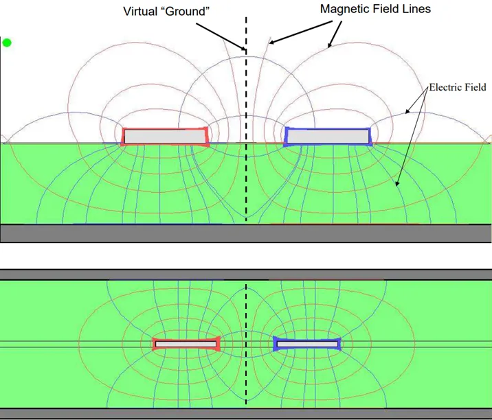
Electromagnetic interference occurs when unintentional coupling generates radiated or conducted noise, often from fast edges creating broadband spectra. Traces with high dv/dt excite far-field radiation, penetrating enclosures if not contained. Ground planes in multilayer boards provide shielding by confining fields, but plane separation dictates effectiveness; closer planes lower loop inductance and emissions.
Crosstalk comprises near-end (forward) and far-end (backward) components, driven by mutual capacitance and inductance between aggressor and victim traces. Capacitive crosstalk dominates in edge-coupled lines, scaling inversely with separation distance. Inductive crosstalk arises from shared magnetic flux, mitigated by orthogonal routing or stitching vias that shorten return currents.
In high-speed regimes, these mechanisms compound with dispersion and attenuation. Dielectric materials with low loss tangent preserve signal fidelity, but thickness modulates coupling strength. Greater dielectric height reduces electric field fringing, dropping crosstalk voltage by orders of magnitude per standard field solver models.
How Thick PCBs Enhance Signal Integrity
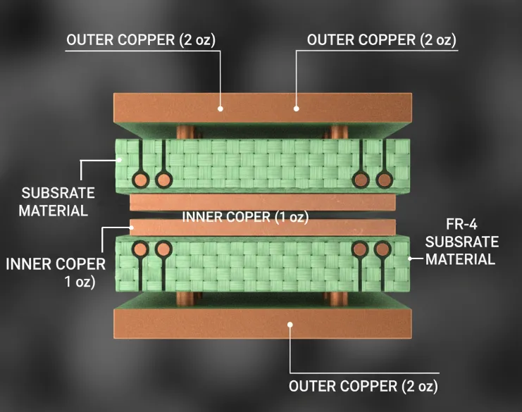
Thick PCBs, typically those exceeding 1.6 mm total height with multilayer construction, fundamentally alter field distributions. Increased core and prepreg thicknesses widen the gap between signal layers and planes, slashing capacitive coupling. For stripline configurations, this separation confines modes, preventing mode conversion that fuels EMI.
Impedance control in thick PCBs relies on consistent dielectric height for predictable characteristic impedance. Microstrip lines on thicker substrates exhibit higher Z0 due to reduced capacitance per unit length, easing matching to driver/receiver specs. Engineers calculate Z0 using formulas where height h directly impacts C = ε0 εr W / h, promoting uniform propagation.
EMI shielding improves as thick structures support interleaved power/ground planes, forming stripline shields that attenuate radiated fields. The plane pair acts as a parallel-plate waveguide, with cutoff frequencies pushed higher by thinner gaps within the stackup, though overall thickness enables more such pairs. This layered shielding confines emissions, aiding compliance without added cans.
Crosstalk reduction follows a 1/d dependency for far-end coupling, where d is dielectric thickness. Doubling d can quarter NEXT/FEXT in symmetric stacks, allowing denser routing without guards. Practical stackups place signals between planes, leveraging thickness for isolation.
IPC-2141A outlines guidelines for controlled impedance in such high-speed boards, emphasizing stackup tolerances.
Best Practices for Thick PCB Design in High-Speed Applications
Start with stackup planning, prioritizing symmetric builds to avoid warpage and maintain uniform thickness. Allocate thicker cores for inner layers to space signals adequately, using 2116 or 7628 prepregs for controlled heights. Simulate stackups early to verify impedance across frequencies, targeting 50 or 100 ohms as needed.
Routing strategies complement thickness: employ length-matched pairs, avoid 90-degree bends, and use differential pairs for common-mode rejection. Stitch ground vias along edges and under traces to minimize slot antennas, enhancing EMI shielding. Maintain 3W spacing minimum between singles, scaling with edge rates.
Material selection favors low-Dk/Df laminates, but thickness uniformity per IPC-2221B ensures repeatability. Vias demand back-drilling in thick boards to stub-resonate discontinuities, preserving integrity. Fabricate prototypes with coupon structures for TDR validation.
Power distribution benefits from dedicated thick planes, reducing ripple that couples as EMI. Decoupling caps near ICs, combined with plane capacitance from close spacing, form effective filters.
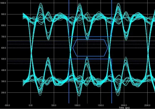
For troubleshooting, eye diagrams reveal crosstalk via eye closure; mitigate by thinning aggressive edges or adding series resistors. EMI scans pinpoint radiators, resolved by thickening local shielding.
Conclusion
Thick PCBs unlock superior signal integrity in high-speed circuits by leveraging physical separation to curb EMI and crosstalk. Strategic stackups, precise impedance control, and adherence to design principles yield robust performance. Electric engineers benefit from these approaches in demanding applications, ensuring reliable data transmission. Embrace thickness as a core tool in your high-speed PCB design arsenal for future-proof designs.
FAQs
Q1: How does thick PCB signal integrity improve crosstalk reduction in multilayer boards?
A1: Thick PCBs increase dielectric separation between traces, inversely scaling capacitive and inductive coupling. This reduces noise injection on victim lines, especially at gigabit speeds. Ground planes adjacent to signals further shield fields, aligning with high-speed PCB design needs. Simulations confirm substantial NEXT/FEXT drops with modest thickness gains.
Q2: What role does EMI shielding play in thick PCB designs for high-speed applications?
A2: EMI shielding in thick PCBs uses interleaved planes to confine radiated fields, lowering emissions. Thicker structures support more shielding layers, acting as low-pass filters for broadband noise. This minimizes external interference susceptibility. Proper via fencing enhances effectiveness without added components.
Q3: Why is impedance control critical in thick PCB signal integrity?
A3: Impedance control prevents reflections that distort waveforms in thick PCBs. Dielectric thickness directly influences Z0, requiring tight tolerances for matching. Consistent stackups ensure uniform propagation delays. This foundation supports crosstalk reduction and EMI mitigation in high-speed circuits.
Q4: How can engineers optimize stackups for crosstalk reduction PCB performance?
A4: Optimize by placing signals in inner layers with thick dielectrics between aggressors. Symmetric builds maintain planarity. Reference IPC guidelines for spacing. Vias and guards provide redundancy. Test iteratively for validation.
References
IPC-2141A — Design Guide for High-Speed Controlled Impedance Printed Boards. IPC
IPC-2221B — Generic Standard on Printed Board Design. IPC
IPC-6012E — Qualification and Performance Specification for Rigid Printed Boards. IPC, 2015


