










PCB Stack-up Design: Mastering Layer Order for Optimal Performance
WHAT THIS VIDEO COVERS
This video dives deep into why PCB stack-up design is far more important than simply counting layers. It explains how the strategic arrangement of signal, power, and ground layers directly impacts the performance and reliability of your printed circuit board.
Key concepts covered include placing signal layers adjacent to ground planes for short return paths, which reduces noise and EMI. The video also highlights how positioning power and ground planes close together creates a built-in plane capacitor that stabilizes voltage rails and lowers PDN impedance — critical for high-speed circuits.
Common configurations are demonstrated, such as the classic Signal-GND-PWR-Signal for 4-layer PCB designs and more advanced alternating patterns for higher layer counts. Consistent layer thickness and prepreg selection are emphasized for maintaining impedance control and manufacturability.
A well-optimized stack-up balances signal integrity, thermal management, and cost. Poor layer ordering often leads to reflections, crosstalk, and power instability. This knowledge is especially valuable when developing PCB prototype boards for high-frequency PCB applications, automotive electronics, medical devices, and industrial control systems.
KEY HIGHLIGHTS
- Strategic Layer Placement: Positioning signal layers next to ground planes provides clean return paths and minimizes EMI and noise.
- Power Delivery Optimization: Close power-ground plane pairs create low-impedance capacitance, stabilizing supply rails for high-speed components.
- Common Stack-up Configurations: Classic 4-layer Signal-GND-PWR-Signal arrangement and multi-layer patterns that balance performance with manufacturability.
Impact on Signal Integrity, EMI, and Power Delivery
Proper PCB stack-up design directly influences electromagnetic compatibility and circuit performance. Signal layers placed adjacent to solid ground planes minimize return path loop inductance, reducing the potential for signal reflections and crosstalk. In high-speed applications, even minor discontinuities in reference planes can introduce noise that propagates through the board.
Power and ground plane proximity enhances planar capacitance, which helps decouple high-frequency noise and supports stable voltage delivery. This is particularly important in designs with fast-switching components, where inadequate PDN impedance can cause voltage droops and timing issues.
From a manufacturing viewpoint, symmetrical copper distribution across layers helps prevent board warpage during lamination and pressing. Factories often encounter issues when stack-ups lack balance, leading to registration errors or uneven thickness that affect final assembly yields.
DFM Considerations for Reliable Stack-up Implementation
In production, stack-up choices must align with fabricator capabilities regarding material availability, press parameters, and tolerance controls. Prepreg types (such as 1080, 2116, or 7628) and core thicknesses significantly influence impedance and overall board thickness. Designers should collaborate early with manufacturers to verify proposed stack-ups against standard processes.
Key DFM recommendations include maintaining symmetric construction to minimize thermal stress and ensuring adequate dielectric spacing for target impedance values (commonly 50Ω single-ended or 90-100Ω differential). Copper balancing is essential—uneven distribution across layers can cause twisting or bowing during high-temperature lamination.
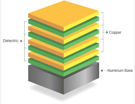
Common Manufacturing Challenges and Solutions
Poor stack-up planning frequently results in issues discovered only during fabrication or testing, such as impedance mismatches, increased EMI in final assemblies, or delamination risks. For example, routing high-speed signals far from reference planes enlarges current return loops, amplifying noise. Split planes under critical traces can also create unintended antennas.
Solutions involve early DFM reviews that include impedance modeling, material selection verification, and prototype validation. Factories recommend grouping similar-frequency signals and providing continuous reference planes where possible. In multilayer builds, tighter registration tolerances for 6+ layers make precise stack-up definition even more critical.
Layer Configuration
| Layer Configuration | Primary Benefits | Common Applications | DFM Notes |
|---|---|---|---|
| Signal-GND-PWR-Signal (4-layer) | Excellent return paths, low PDN impedance, good EMI control | High-speed digital, automotive, industrial | Symmetrical copper; verify prepreg for impedance |
| GND-Signal-Signal-GND | Superior shielding, reduced crosstalk | RF/mixed-signal, medical devices | Ensure no adjacent high-speed signals without reference |
| Multi-layer (6-12) with alternating planes | Enhanced isolation, better thermal/ power handling | Complex IoT, aerospace | Copper balance critical to avoid warpage |
FAQ
Q1: What is the best layer order for a 4-layer PCB?
A1: The most common and effective stack-up is Signal-GND-PWR-Signal. This provides excellent return paths for signals and good power distribution while maintaining reasonable manufacturing cost.
Q2: How does PCB stack-up affect signal integrity and EMI?
A2: Proper stack-up with signal layers adjacent to ground planes creates short return paths, reducing loop inductance, crosstalk, and electromagnetic interference. Poor arrangement leads to reflections and signal degradation.
Q3: When should you invest more effort in advanced PCB stack-up design?
A3: You should prioritize detailed stack-up planning for high-speed designs, impedance-sensitive circuits, multilayer boards (6+ layers), or applications in medical, automotive, and aerospace where reliability is non-negotiable.
Q4: What are typical failure modes from suboptimal stack-up in production?
A4: Common problems include board warpage from copper imbalance, registration shifts in multilayer pressing, and EMI failures during compliance testing. These often stem from inadequate plane continuity or excessive layer transitions, leading to costly respins and delayed time-to-market.
Q5: How can designers ensure stack-up compatibility with fabrication processes?
A5: Provide detailed stack-up drawings specifying copper weights, dielectric materials, and target impedances. Manufacturers perform DFM analysis to confirm feasibility, recommending adjustments for standard panel sizes and press capabilities to optimize yield.
This is a PCB — but do you know how the layers are arranged?
The order of power, signal, and ground layers can make or break your design.
Place signal layers close to a ground plane.
That gives your signals a short, clean return path — reducing noise and EMI.
Placing power and ground planes close together creates a large plane capacitor — lowering PDN impedance and stabilizing supply rails for high‑speed devices.
For a typical 4‑layer board we often use: signal-ground-power-signal is a classic stack-up.
For more layers, alternate signal and power: GND-SIG-PWR-SIG-GND-PWR.
Keep layer thickness and prepreg consistent to maintain impedance control.
A well-designed stack-up balances signal integrity, power stability, and manufacturability.
Bad layer order? Expect reflections, noise, and voltage fluctuations.
Hope this helps! Check our blog for more — and sign up to unlock your $1 PCB prototype at AIVON!





