










In PCB design, impedance determines whether a signal can travel the line in a stable way. If impedance matching is ignored, reflection and crosstalk appear and debug stalls. The calculation itself follows a fixed logic: gather the stack-up parameters, choose the model, then run the tool. The flow below covers the models, the required inputs, laminate data, and a worked 6-layer example.
Why Impedance Must Be Calculated
When voltage and current travel on a transmission line, a mismatch in characteristic impedance behaves like sound hitting a wall: part of the energy comes back as a reflection. In signal integrity, reflection, crosstalk, and cuts in a power plane are, at root, impedance discontinuities.
On high-frequency and high-speed boards, a mismatch affects transmission speed and stability and can make the product fail. Calculating the line so that the target impedance is met is a required step in the design, not an optional one.
Three Impedance Models: Inner Layer versus Outer Layer
Before running a calculation, choose the model. Polar SI9000 is built around three model families, each with inner-layer and outer-layer versions:
- Characteristic impedance: outer-layer characteristic impedance, inner-layer characteristic impedance
- Differential impedance: outer-layer differential impedance, inner-layer differential impedance
- Coplanar impedance: outer-layer coplanar characteristic impedance, inner-layer coplanar characteristic impedance, outer-layer coplanar differential impedance, inner-layer coplanar differential impedance
Seven Required Inputs and Six Factors That Move the Result
Impedance calculation is not a matter of filling arbitrary numbers. The required parameters must be known first, then the factors that shift the result.
1. Seven Required Inputs
These seven values must be available before the calculation:
- Board thickness: overall finished PCB thickness
- Layer count: including signal layers and power layers
- Laminate: for example FR-4 or Rogers
- Surface finish: gold plating, HASL, and similar
- Target impedance: the design goal (for example 50 Ω or 90 Ω)
- Impedance tolerance: allowed error (for example ±10%)
- Copper weight: inner- and outer-layer foil thickness (1 oz = 0.035 mm)
2. Six Factors That Affect Impedance
Meaning of each term:
- H1: dielectric thickness (prepreg or core, copper thickness not included)
- Er1: dielectric constant (use an average when several prepregs or cores are pressed together)
- W1: bottom width of the impedance trace; W2: top width of the impedance trace
- T1: finished copper thickness
- Cer: solder-mask dielectric constant (fixed value 3.3)
- C1: solder-mask thickness over the laminate (usually taken as 0.8 mil)
- C2: solder-mask thickness over copper / traces (usually taken as 0.5 mil)
- Zo: calculated theoretical impedance
3. Top and Bottom Trace Widths
W1 and W2 are not fixed. They shift with copper weight and process. Use the table below when entering widths.
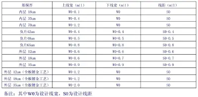
Note: W0 is the designed trace width and S0 is the designed spacing. The offset from W0 depends on copper weight and process.
Laminate Data: FR-4 and Rogers
Dielectric constant and thickness are the main material inputs. Values differ widely by laminate. Common data used in calculation are collected below.
1. Standard FR-4 Core: Shengyi and Equivalent Materials
FR-4 is the most common laminate. Thickness (mm / mil) versus dielectric constant for Shengyi FR-4 cores is shown below. Choose the core from the required board thickness.

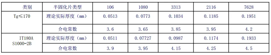
2. Prepreg: Common Styles Have Fixed Data
Prepreg is the bonding layer in lamination. Typical styles and thicknesses:
- Style 106: thickness 0.04 mm
- Style 1080: thickness 0.06 mm
- Style 2116: thickness 0.11 mm
- Style 7628: thickness 0.19 mm
Detailed parameters are in the table below.
3. Rogers Laminates for High-Frequency Boards
High-frequency PCBs often use Rogers material, which has a stable dielectric constant. Key values:
- Rogers 4350: dielectric constant 3.36 at 0.1 mm thickness; 3.48 at other thicknesses
- Rogers 4003: dielectric constant 3.38
- Rogers 4403 prepreg: dielectric constant 3.17
4. Lamination Rules
A multilayer board is pressed from cores and prepreg. Four rules reduce layer slip and poor appearance:
- Do not stack four or more prepreg sheets. The stack is prone to slip (layer misregistration).
- Do not place style 7628 prepreg on the outer dielectric. The coarse surface hurts appearance.
- Do not place three sheets of style 1080 prepreg on the outer dielectric. That stack also tends to slip.
- Core thickness ≥ 0.11 mm. Use two cores on a 6-layer board and three cores on an 8-layer board.
Measured Thickness Is Not Theoretical Thickness
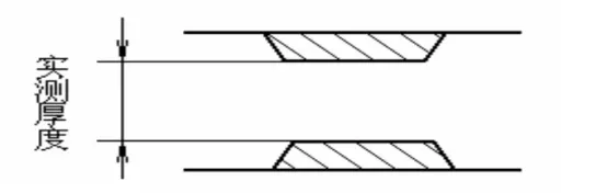
The theoretical stack-up thickness and the measured thickness differ because of copper weight and residual copper percentage.
1. Residual Copper Percentage
Residual copper percentage is copper area on the layer divided by the full board area:
- Unprocessed raw material: 100%
- Fully etched bare laminate: 0%
- Power and ground planes: typically 70%
- Signal layers: typically 23%
- Outer layers: take 1 (full copper coverage as the default)
2. Measured-Thickness Formula
Measured thickness = theoretical thickness − copper thickness 1 × (1 − X1) − copper thickness 2 × (1 − X2), where X1 and X2 are the residual copper percentages of the corresponding layers. Copper thickness uses 1 oz = 0.035 mm.
The difference between theoretical and measured thickness is shown below.
Worked Example: Impedance Calculation on a 6-Layer Board
The following 6-layer example runs from requirements through stack-up to the tool result.
1. Design Requirements
- Board thickness: 1.2 mm (allowed error ±0.12 mm)
- Laminate: FR-4
- Layer count: 6
- Copper: inner layers 1 oz, outer layers 0.5 oz
- Target impedance: 50 Ω single-ended on the outer layer; 90 Ω differential on an inner layer
2. Stack-up
Using core and prepreg data and the thickness target, the 6-layer stack-up is shown below with the key dimensions marked.
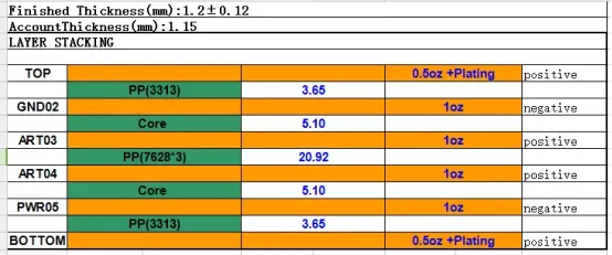
Measured prepreg thickness
- PP (3313) measured = 0.1034 mm (theoretical) − 0.035 / 2 mm × (1 − 1) (outer 0.5 oz, residual copper 1) − 0.035 mm × (1 − 0.7) (inner 1 oz, residual copper 70%) = 0.0929 mm = 3.65 mil
- PP (7628 × 3) measured = 0.1951 × 3 mm (theoretical) − 0.035 × (1 − 0.23) (inner 1 oz, signal-layer residual copper 23%) × 2 = 0.5314 mm = 20.92 mil
Total thickness check
Board total thickness = 0.5 oz + 3.65 mil + 1 oz + 5.1 mil + 1 oz + 20.92 mil + 1 oz + 5.1 mil + 1 oz + 3.65 mil + 0.5 oz = 1.15 mm, which meets 1.2 ± 0.12 mm.
3. Outer-Layer 50 Ω Single-Ended Line in SI9000
Open SI9000, select the outer-layer characteristic-impedance model, and enter the stack-up values (H1 = 3.65 mil, Er1 = 3.85, T1 = 0.69 mil, and the remaining fields). The calculated theoretical width is W0 = 6.8 mil.
For easier routing, the width can be adjusted. At 5.5 mil, Zo = 54.82 Ω, which lies inside 50 Ω ± 10% (45–55 Ω) and meets the spec.
Tool screens
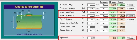
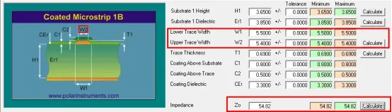
5. Result Summary
All impedance results for the design are collected below.
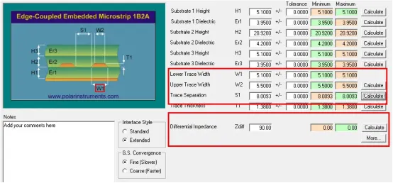
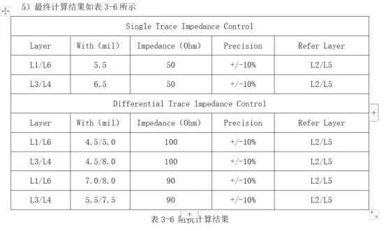
Summary
Impedance calculation is a standard sequence: gather parameters, choose the model, run the tool, then trim width to the tolerance. The meaning of each input, the laminate data, and the lamination rules above are what make that sequence repeatable.






