The fabrication drawing specifies 1.6 mm, but the finished board measures 1.44 mm with a caliper. Nothing appears to be wrong, yet the result is still unsettling.
This does not necessarily mean that the fabricator used inferior materials. From the initial design to the finished PCB, every micrometer of thickness is affected by material behavior and the lamination process.
Many engineers have encountered the same situation. The fabrication drawing specifies "Board Thickness: 1.6 mm ±10%," but the delivered board measures 1.44 mm—exactly at the lower limit. It is natural to wonder whether the stackup was entered incorrectly or whether the fabricator substituted a cheaper material.
The actual explanation is that the 1.6 mm value on the drawing is not an exact physical value. It is a target thickness. From the raw materials through lamination, every layer expands, compresses, shrinks, or flows. The final board thickness is not simply an exact value calculated from a list of nominal material thicknesses. It is the result of the balance reached by the materials during the lamination process.
A PCB Is Not a Solid Slab—It Is a Layered Structure
A multilayer PCB is built from three primary material categories.
Core
The core is a rigid laminate with copper foil already bonded to both sides. It forms the structural framework of the board and has relatively stable thickness characteristics. The incoming-material tolerance from the supplier is generally within ±10%.
Prepreg
Prepreg, or PP, consists of glass fabric impregnated with partially cured resin. It functions as both the bonding material and the dielectric layer between adjacent layers. Before lamination, prepreg has a specified nominal thickness. During lamination, however, the resin melts, flows into the spaces between copper features, and then cures. Its final thickness can therefore be significantly lower than its nominal thickness.
Copper Foil
Inner-layer copper foil is etched to form circuitry. The copper on the outer layers is also subjected to pattern plating, so its final thickness can increase during fabrication. One ounce of copper has an original thickness of approximately 35 μm. After plating and surface finishing, the final copper thickness on an outer layer may increase by nearly another ounce.
During stackup construction, these materials are arranged in a sequence such as copper foil, prepreg, core, prepreg, copper foil, and so on. The stack is then consolidated into a single structure under elevated temperature and pressure. In practical terms, finished board thickness is the total distance from the surface of the top copper layer to the surface of the bottom copper layer after lamination.
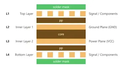
The Core Formula: Copper Thickness + Laminated Prepreg + Core Thickness
The basic calculation is straightforward:
Finished board thickness ≈ 2 × outer-layer copper thickness + Σ laminated prepreg thickness + Σ core thickness
The difficult part is determining the laminated thickness of the prepreg. Its final thickness is not equal to the nominal thickness printed in a material table:
Laminated prepreg thickness = theoretical prepreg thickness ? lamination loss
The lamination loss is strongly affected by the copper distribution on the inner layers. Where inner-layer copper has been etched away, resin must flow into the resulting spaces. If the routing is sparse and the copper distribution is low, more empty space must be filled. More resin flow generally means a greater reduction in the final prepreg thickness.
Consider the following simplified four-layer example:
- Top-layer copper foil: 1 oz, approximately 35 μm
- Prepreg, 2116 × 2: theoretical total thickness of approximately 0.21 mm; with a 50% copper distribution, the lamination loss is approximately 0.018 mm, producing a final thickness of approximately 0.192 mm
- Core: 0.5 mm
- Bottom-side prepreg: same as the top-side prepreg, approximately 0.192 mm
- Bottom-layer copper foil: 1 oz, approximately 35 μm
The resulting thickness is approximately:
0.035 + 0.192 + 0.5 + 0.192 + 0.035 = 0.954 mm
If the nominal design target is 1.0 mm, the calculated result is 0.954 mm. This falls within a ±10% tolerance range and is therefore acceptable under that tolerance.
Now consider what happens when the inner-layer copper distribution increases from 50% to 90%. The lamination loss is reduced because less resin must flow into large etched areas. The actual prepreg thickness increases, and the total board thickness may approach or even exceed 1.0 mm. The material list has not changed, but the copper distribution has. As a result, the finished thickness can differ by more than 0.1 mm.
Why Do Finished Boards Often Tend to Be Thin?
Three process-related mechanisms can cause a board to trend toward the lower side of its specified thickness range.
1. Resin Flow Is Irreversible
During lamination, resin flows into the gaps between inner-layer traces. After cooling and curing, the resin becomes solid, but the material that flowed into those spaces no longer contributes to the original uncompressed prepreg thickness. The lower the copper distribution, the more resin may be displaced or redistributed, and the greater the potential reduction in final dielectric thickness.
This is why prepreg thickness cannot be evaluated independently of the copper pattern. A stackup that works for a dense copper area may produce a different dielectric thickness in a region with sparse routing.
2. The Nominal Outer Copper Thickness Can Be Misleading
The "1 oz" value listed in a stackup commonly refers to the original copper foil thickness supplied with the laminate. After outer-layer imaging, pattern plating, etching, and surface finishing, the final copper thickness may increase by nearly another ounce.
This additional plated copper is sometimes overlooked during a theoretical thickness calculation. The fabricator, however, must account for it when controlling the actual production process. Consequently, the relationship between the nominal stackup and the measured board thickness may not be obvious if only the original foil thickness is considered.
3. The Process Window Can Push the Target Toward the Lower Limit
For a general ±10% thickness tolerance, a 1.6 mm board may be accepted between 1.44 mm and 1.76 mm. To control yield and avoid downstream assembly problems, a fabricator may set the lamination target toward the middle or lower part of the allowed range.
A board that is too thick can interfere with connector insertion, card-edge engagement, or enclosure assembly. A board that is slightly thin may be less likely to create those mechanical interference problems, provided that it remains within the specified tolerance. This process tradeoff can explain why a board measuring close to the lower limit is not automatically evidence of poor workmanship.
A Counterintuitive Detail: Gold-Finger Thickness Is Defined Differently
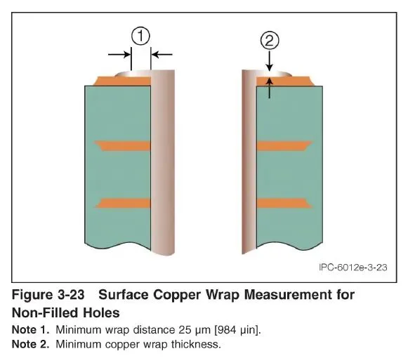
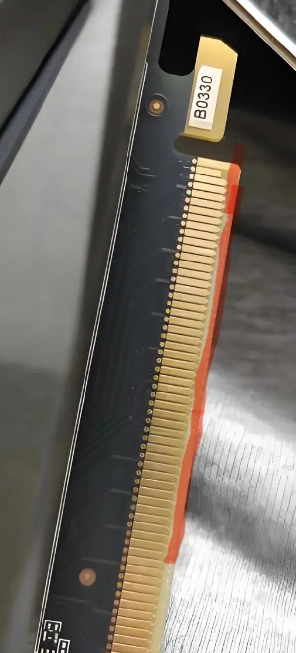
For gold-finger boards, IPC-6012 provides a special definition for finished board thickness. The thickness is measured in the gold-finger area, excluding the solder mask but including the plated copper associated with the surface finish. For areas without gold fingers, finished board thickness includes the solder mask thickness.
This means that the definitions applied to the gold-finger region and the ordinary PCB region are not identical. Measurements from the two areas may differ by several tens of micrometers, even on the same board.
If a card-edge slot or connector clearance is designed using the thickness of a standard solder-mask-covered region, the gold fingers may fit too loosely or too tightly. This distinction is easy to overlook when designing edge connectors and mechanical interfaces. The thickness requirement for the gold-finger region should therefore be stated explicitly in the fabrication documentation.
Practical Design Recommendations
1. Do Not Treat the Stackup Calculation as an Exact Thickness Guarantee
Specify the target thickness and its tolerance rather than demanding an unrealistic exact value. The fabricator will normally adjust the material combination and lamination process according to available prepreg types, lamination parameters, and the copper distribution of the design.
2. Use Copper Distribution to Guide Prepreg Selection
When the copper distribution in a region is below 50%, the prepreg construction may need to be adjusted. This can involve increasing the number of prepreg sheets or selecting a material with a higher resin content, such as 1080. Otherwise, the final dielectric thickness after lamination may become too small and affect controlled impedance.
3. Specify Gold-Finger Thickness Separately
For gold-finger boards, clearly define the thickness tolerance for the gold-finger region on the fabrication drawing. The drawing should also state whether the specified value excludes the solder mask. This avoids ambiguity between the mechanical thickness requirement and the general finished-board thickness requirement.
4. Lock Down Dielectric Thickness Around Critical Impedance Layers
Overall board thickness may be allowed to vary by ±10%, but the dielectric thickness between the copper layers that define a controlled-impedance structure is more critical. If that dielectric spacing changes significantly, a nominal 50 Ω trace may shift to approximately 45 Ω or 55 Ω, causing a controlled-impedance or TDR test to fail.
For this reason, a stackup should not be evaluated only by its total thickness. The thickness and material properties of the dielectric layers around critical signal layers must also be controlled. In high-speed designs, the relationship between trace geometry, copper thickness, dielectric thickness, and resin distribution directly affects the final impedance.
Board Thickness Is a Process Result, Not Just a Calculation
PCB thickness calculations deal with the physical uncertainty of materials and manufacturing processes. The designer calculates a theoretical stackup, while the fabricator controls a practical process window. The delivered board is the result of these two factors reaching a workable balance.
Understanding this relationship is more useful than memorizing a single thickness formula. A nominal 1.6 mm board is a target built from cores, prepreg, copper foil, plated copper, copper distribution, resin flow, and lamination control. Once these factors are considered together, a measured value such as 1.44 mm is no longer mysterious: it is the lower boundary of the specified process window, not necessarily a manufacturing error.