Copper wrap plating refers to the region where the copper plating on a through-hole wall extends outward at the hole entrance and forms a continuous metallic structure with the copper foil on the outer layer.
This feature is evaluated using two dimensions:
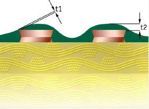
- Wrap thickness: the thickness of the copper layer in the wrapped region at the hole entrance.
- Wrap length: the effective distance over which the plated copper extends from the hole wall onto the outer-layer copper foil while maintaining a continuous connection.
These two measurements confirm whether the plated through-hole wall and the outer-layer copper foil form a continuous copper structure with sufficient thickness and sufficient extension distance. The requirement is therefore related to structural integrity and long-term reliability, not merely to the visual appearance of the hole entrance.
How Does the IPC Standard Define Copper Wrap Plating?
IPC-6012E defines copper wrap plating as part of the quality requirements for plated through-holes. The standard distinguishes between the thickness of the wrapped copper and the length of the continuous wrap. Both dimensions must be considered because they describe different aspects of the connection between the hole-wall plating and the outer-layer copper.

Figure 1 | Copper wrap plating definition in IPC-6012E

Figure 2 | Parameters used to evaluate copper wrap thickness and wrap length

Figure 3 | Continuous copper structure between the plated through-hole wall and outer-layer copper
Why Is Continuous Coverage at the Hole Entrance Important?
As the copper plating on a through-hole wall extends toward the outer layer, it passes through a geometric transition region. Inside the hole, the copper exists as wall plating. At the hole entrance, that plating must connect smoothly to the outer-layer copper foil. This region is affected by both manufacturing conditions and the mechanical and thermal environment experienced by the finished PCB, making it an important location for through-hole reliability.

Figure 4 | Mechanical stress concentration in the copper wrap transition region
If the copper wrap is too thin, the local metallic cross-section is reduced. If the wrap length is too short, the effective continuous connection between the hole-wall copper and the outer-layer copper foil is limited. In either case, mechanical stress becomes concentrated in a relatively small area.
IPC defines both wrap thickness and wrap length because the objective is to control the integrity of the metal structure at the hole entrance. A through-hole can have adequate average wall-plating thickness while still having an inadequate connection to the outer-layer copper. Conversely, the connection may extend far enough but remain too thin to withstand long-term stress. Evaluating only one dimension cannot fully represent the reliability of the entire structure.
What Does Insufficient Wrap Thickness Affect?
Mechanical Reliability
Copper has mechanical strength and must withstand the forces applied during PCB handling, assembly, and use. When the copper in the wrap region is too thin, its ability to carry local mechanical stress decreases. The reduced cross-section creates a structurally weaker area that is more sensitive to deformation and mechanical loading.
Thermal-Cycling Reliability
During operation, a PCB may repeatedly experience heating and cooling. The substrate material and copper have different thermal expansion characteristics, so the plated through-hole structure is subjected to repeated thermomechanical stress.
A locally thin wrap region is more likely to develop stress concentration. Over many thermal cycles, this concentration can initiate a microcrack. The crack may gradually propagate through the copper structure and eventually interrupt the electrical connection of the plated through-hole.
- Insufficient wrap thickness: increases the risk of a locally weakened copper structure, thermal-cycle cracking, and mechanical failure.
- Insufficient wrap length: increases the risk associated with an inadequate continuous connection between the hole-wall copper and the outer-layer copper foil.
- Insufficient thickness and length at the same time: further increases the risk to long-term through-hole reliability.
Wrap thickness therefore controls the local copper structure's resistance to cracking and its ability to tolerate thermal cycling. It is not simply a dimensional feature used for visual inspection.
What Does Insufficient Wrap Length Affect?
Wrap length controls the effective continuous connection area between the plated through-hole wall and the outer-layer copper foil. Even when the copper thickness is sufficient, a very short continuous wrap provides only a limited area for transferring mechanical stress between the two copper structures.
When the connection area is too short, stress is concentrated within a smaller region. Long-term thermal cycling, mechanical vibration, board bending, and assembly-related forces can then make this high-stress region more susceptible to crack initiation.
In practical terms, wrap thickness determines whether the copper itself has sufficient structural strength, while wrap length determines whether the copper structures have a sufficiently long and continuous connection. Both dimensions contribute to the reliability of the plated through-hole.
Why Is Hole-Wall Copper Thickness Alone Not Enough?
This is one of the main reasons that copper wrap plating is defined separately. Consider a through-hole whose average wall-plating thickness meets the applicable requirement, but whose copper does not extend sufficiently onto the outer-layer copper foil at the hole entrance. The average wall thickness may appear acceptable, while the continuity of the hole-entrance structure remains inadequate.
The reverse situation is also possible. The copper may extend over a sufficient length, but a local section of the wrap may be too thin. That weak section may crack during thermal cycling even though the overall connection length is adequate.
Controlling only the average wall-plating thickness therefore does not fully represent through-hole structural reliability. The purpose of also controlling copper wrap plating is to verify that the plated hole wall, the wrapped region, and the outer-layer copper foil form a complete continuous metal path with sufficient structural strength.
How Can Copper Wrap Plating Affect Electrical Performance?
The most direct effect is the reliability of electrical continuity. A through-hole provides an electrical path between different PCB layers. If a crack develops in the wrap region or if part of the copper separates from the outer-layer foil, the connection may initially remain electrically continuous.
For this reason, a standard production electrical test may not always detect the problem at the beginning of its development. As the crack grows during long-term use, however, the connection may exhibit intermittent continuity, increased contact resistance, electrical noise, or eventual open-circuit failure.
This failure mode has an important characteristic: initial electrical testing may be normal even though long-term reliability is inadequate. Electrical continuity testing alone is therefore not sufficient to evaluate the complete quality of a plated through-hole. Cross-sectional inspection and dimensional verification are also needed to assess the physical copper structure.
Which Manufacturing Factors Can Cause Insufficient Copper Wrap?
Copper wrap defects are usually not caused by one isolated process step. Several manufacturing conditions can affect the shape, thickness, adhesion, and continuity of the copper at the hole entrance. Potential causes include:
- Poor hole-entrance geometry after drilling.
- Resin residue or other contamination on the hole wall.
- Insufficient pretreatment, resulting in poor adhesion of subsequent copper layers.
- Nonuniform electroless copper deposition.
- Uneven current distribution during electroplating.
- Insufficient plating capability inside high-aspect-ratio through-holes.
- Local reduction of the copper structure during subsequent etching.
- Dimensional changes caused by the laminate material or the lamination process.
- Misalignment between process steps, causing displacement of the hole-entrance structure.
These factors can affect either the local copper thickness, the extension of the plating onto the outer layer, or the continuity between the two copper regions. Process control must therefore consider the complete chain from drilling and hole cleaning through copper deposition, electroplating, etching, lamination-related dimensional variation, and alignment.
Key Takeaway
The critical question is not merely whether a through-hole has electrical continuity or whether its average wall-plating thickness meets a requirement. The hole-wall copper must form a sufficiently thick, sufficiently long, and continuous metal structure with the outer-layer copper foil.
Wrap thickness controls the strength and crack resistance of the local copper cross-section. Wrap length controls the effective continuous connection area between the hole-wall plating and the outer-layer copper. Together, these requirements help the plated through-hole withstand the thermal and mechanical stresses generated during PCB manufacturing, assembly, and product operation.