The distance between PCB gold fingers and the board outline directly affects manufacturing yield, mechanical insertion and removal, electrical performance, and long-term reliability. A clearance that is either too small or too large creates different application risks. Selecting an appropriate distance is therefore an important prerequisite for achieving stable production and reliable field performance.
Impact on PCB Manufacturing
When the Clearance Is Too Small
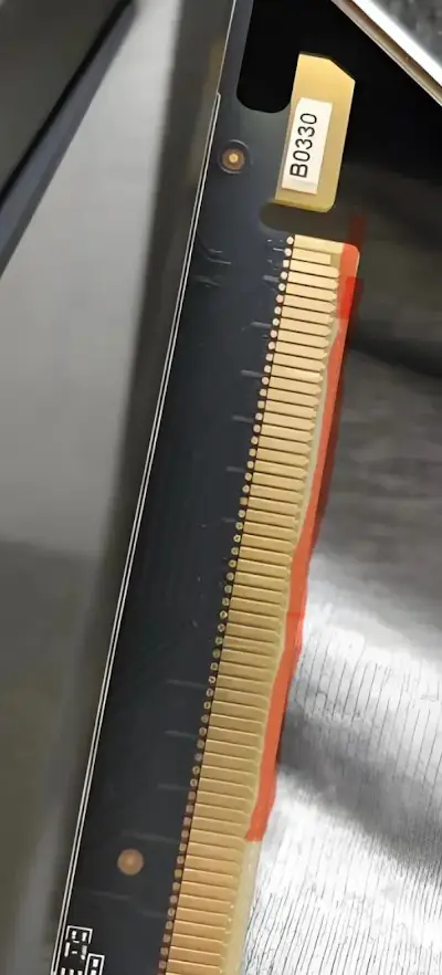
If the distance between the gold fingers and the board edge is less than 0.5 mm, the board may be exposed to significant manufacturing risk. PCB profiling tools typically have machining tolerances of approximately ±0.1 mm. With insufficient clearance, the routing bit can easily cut into the edge of the gold fingers, damaging the plating and exposing the underlying copper. The resulting defect can increase the scrap rate of the complete panel to more than 15%.
The edge-beveling operation creates an additional risk. A bevel cut removes material from the board edge and can shorten the effective contact length of the gold fingers. If the remaining contact area does not meet the requirements of the mating connector, the finished board may fail during assembly even if the plating itself appears visually acceptable.
When the Clearance Is Too Large
An excessive distance generally does not create an immediate manufacturing scrap risk. However, it consumes usable PCB area and reduces the space available for routing. On high-density interface boards, the routable area may decrease by approximately 10% to 20%. This can make escape routing and signal placement more difficult and indirectly increase manufacturing pressure on the circuit pattern.
For applications that require automated beveling, a clearance of at least 0.5 mm can support stable processing. Under the conditions described for memory modules, graphics cards, and industrial backplanes, this spacing allows the gold-finger plating to remain intact and can support a plating-integrity yield above 99% in high-volume production.
Impact on Mechanical Insertion and Removal
Insufficient Clearance
When the clearance is too small, beveling may leave insufficient effective contact length at the end of the gold fingers. During insertion, the board may not align correctly with the connector contacts, causing positional deviation and unstable insertion force. The insertion-force deviation may exceed ±5 N.
Repeated insertion and removal under these conditions can accelerate wear of the connector spring contacts. In the described application case, the overall insertion/removal life may fall from a nominal 5,000 cycles to fewer than 1,000 cycles. The risk is not limited to connector wear: damage to the gold-finger edge can also reduce contact stability over time.
Excessive Clearance
If the gold fingers are positioned too far inward from the board edge, their location may no longer match the contact travel and locking geometry of the mating connector. The board may fail to enter the connector completely or may not reach the intended locking position. This can result in looseness, incomplete contact, or intermittent connection.
Vibration makes this problem more serious. A connector that does not fully engage the intended contact and locking position can experience momentary signal or power interruptions when the assembly is subjected to mechanical shock or vibration.
Mechanical Design Considerations
A commonly stated design principle is to select the distance according to at least 1.5 times the PCB thickness. With an appropriate bevel, this relationship allows the gold fingers to mate fully with the connector spring contacts and helps keep insertion force within the required range. It is also intended to support long mechanical service life for interfaces such as PCIe and DDR, including applications described as requiring million-cycle-level mechanical endurance.
The exact value should still be verified against the connector geometry, board thickness, bevel angle, insertion depth, and specified insertion/removal force. The clearance alone cannot compensate for a mismatch between the PCB edge profile and the connector design.
Impact on Electrical Performance
Effects of Edge Damage and Oxidation
If the gold-finger edge is cut during profiling or beveling, the exposed copper underneath the plating can oxidize. In the stated application case, contact resistance may increase from less than 20 mΩ to more than 100 mΩ. Such an increase can degrade both power delivery and signal quality.
For high-speed interfaces such as PCIe 5.0 and DDR5, unstable contact resistance can increase insertion loss and disturb the electrical interface. The possible consequences include packet errors, link-speed reduction, or failure of the device to complete identification. The mechanism is particularly important where the gold fingers carry both high-speed differential signals and supply or ground connections.
Effects of Excessive Trace Length
An excessively large edge clearance can force the traces leading to the gold fingers to become longer. The additional routing length increases the parasitic inductance and capacitance associated with the high-frequency path. At data rates above 25 Gbps, these additional parasitics can introduce extra signal loss and reduce the available transmission bandwidth.
For this reason, electrical design must balance two opposing requirements. The clearance must be large enough to protect the gold-finger plating during profiling and beveling, but it should not be unnecessarily large because the resulting trace extension can degrade high-speed signal performance.
Plating and Current-Carrying Requirements
Within the stated conventional clearance range of 0.5 mm to 3 mm, maintaining complete plating without oxidation helps keep contact resistance stable. The described design target supports current transmission of up to 15 A and is intended for applications such as optical modules and industrial control boards that require both reliable contact and relatively high power transfer.
These values should be treated as application-specific design targets rather than universal limits. Actual performance also depends on the plating structure, contact force, connector material, surface contamination, operating environment, and the current distribution across adjacent contacts.
Impact on Long-Term Reliability
Environmental Corrosion
A damaged gold-finger edge no longer has complete plating protection. In salt spray or high-humidity environments, the exposed metal can corrode rapidly. Under the stated 96-hour salt-spray test condition, visible corrosion may occur at damaged locations. This can make the board unsuitable for long-term use in aerospace, outdoor industrial equipment, and other demanding environments.
Mechanical Stress at the Gold-Finger Root
When the gold-finger region is positioned too far inward, the supporting PCB material near the root of the fingers may be insufficient for the required mechanical load. Repeated insertion and removal can then cause bending stress to concentrate at the gold-finger root. Over time, the associated circuit traces may crack or break.
The stated application case associates this condition with a reduction in mean time between failures (MTBF) of more than 30%. Adequate substrate support near the board edge is therefore important not only for initial connector engagement but also for resistance to repeated mechanical loading and vibration.
For higher-reliability applications, an additional process allowance of 0.2 mm beyond the standard safety clearance is recommended in the described design approach. This extra margin is intended to improve tolerance to profiling variation and help the finished board pass vibration and corrosion testing.
Design Principles for Gold-Finger Edge Clearance
Prioritize Manufacturing Safety
- For conventional designs, the minimum distance should not be less than 0.5 mm. In high-precision thin-board applications, the stated lower limit is 0.2 mm. This allowance is intended to accommodate the approximately ±0.1 mm profiling-tool tolerance and prevent direct damage to the gold-finger plating.
- The clearance should exceed the required bevel depth. For example, with a 45° bevel on a 1.6 mm-thick PCB, the bevel depth is approximately 0.55 mm. The gold fingers should therefore be positioned farther from the board edge than this value to prevent the beveling operation from cutting into the contact area.
Protect Mechanical Reliability
- After beveling, the design should retain an effective gold-finger contact length of at least 1.0 mm so that the connector contacts have sufficient engagement travel.
- The bevel and edge clearance should allow the gold fingers to mate completely with the connector contacts. This helps keep insertion force within the specified range and supports the stated mechanical life target of more than 5,000 cycles.
- Sufficient PCB substrate should remain between the gold-finger roots and the board edge. This support reduces the risk of trace bending and fracture during repeated insertion, removal, and vibration.
Control Electrical Performance
- Maintain sufficient clearance to prevent edge damage and copper exposure during profiling. Complete plating helps keep contact resistance below the stated 20 mΩ target for high-speed signaling and high-current transmission.
- Avoid unnecessarily large clearances that extend the gold-finger routing path. Shorter high-frequency paths reduce parasitic inductance and capacitance and help limit additional loss in applications above 25 Gbps.
- Apply the required gold-finger keep-out region. Vias, exposed openings, and unnecessary copper features should not be placed within the gold-finger area, because they can contribute to uneven plating, unintended shorts, or other manufacturing defects.
The distance between a PCB gold finger and the board outline is therefore a combined manufacturing, mechanical, electrical, and reliability parameter. A successful design must account for profiling tolerance, bevel depth, connector geometry, effective contact length, high-speed routing, current capacity, environmental exposure, and long-term mechanical stress. Establishing the clearance from these interacting requirements provides a more reliable basis for both high-volume production and demanding field applications.