The wide range of PCB copper thicknesses results from the interaction between the inherent characteristics of PCB manufacturing processes and the diverse requirements of product design. The reasons can be understood from two perspectives: what the manufacturing process can produce and what the application requires.
Basic Concepts: Base Copper and Finished Copper
Base Copper Thickness
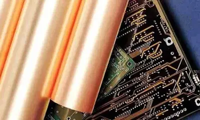
Base copper thickness is the original thickness of the copper foil on the copper-clad laminate when it leaves the laminate manufacturing process. It is the physical starting point for all subsequent PCB processes, including etching and electroplating.
For a multilayer PCB, the base copper usually becomes the copper thickness of the inner-layer circuitry. Once the inner-layer copper has been etched and the layer has been laminated into the board, its thickness is essentially fixed. The finished inner-layer copper thickness is therefore approximately equal to the original base copper thickness, with only a very small amount of material removed during processing.
Finished Copper Thickness
Finished copper thickness is the total copper thickness remaining on the circuit surface after the PCB has completed all relevant manufacturing processes, such as etching, electroless copper deposition, panel plating, pattern plating, and surface finishing. It is the final copper specification delivered to the customer.
The term is especially important for outer-layer circuitry because the outer layers are usually increased in thickness through plating. In simplified form:
Finished outer-layer copper thickness ≈ base copper thickness + electroplated copper thickness
When a customer specifies “1 oz outer-layer copper,” the requirement generally refers to a finished copper thickness of approximately 1 oz, or about 35 μm. The distinction between base copper and finished copper must therefore be made clearly during both PCB fabrication and impedance-controlled design.
Manufacturing Factors: Why Copper Thickness Changes
From the manufacturing perspective, the key principle is that the process flow itself creates a difference between the starting copper thickness and the final copper thickness. Inner and outer layers do not undergo exactly the same sequence of operations, which is why their copper-thickness behavior is different.
Inner-Layer and Outer-Layer Processing
Inner-layer circuitry is generally etched and defined before lamination. After the patterned layer is pressed into the multilayer stackup, it is no longer exposed to the same plating operations used on the outer layers. As a result, the finished inner-layer copper thickness is approximately equal to the starting base copper thickness.
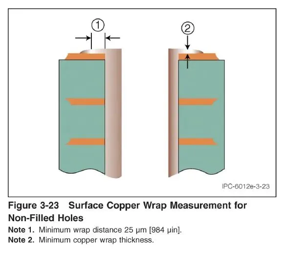
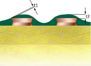
Outer-layer processing is different. After drilling, the hole walls must receive electroless copper and electroplated copper to establish a conductive connection between layers. During this operation, copper is deposited not only on the hole walls but also across the outer-layer surface. The outer-layer copper thickness therefore becomes the base copper thickness plus the plated copper thickness.
This additional plating is necessary for reliable plated-through-hole performance. For example, the source specifies a hole-copper requirement of at least 20 μm for an IPC Class 2 application. Meeting such a requirement often means that the outer layers must be plated beyond the original laminate copper thickness.
Why Thick-Copper Manufacturing Is More Difficult
Increasing copper thickness does not simply involve adding more material. Thick copper introduces challenges throughout the manufacturing process. During etching, the greater copper thickness increases the difficulty of removing unwanted copper cleanly. Lateral etching, or undercut, can become more pronounced, making the final line width and spacing harder to control.
Thick copper can also affect lamination quality. The large copper features and greater copper volume may make it more difficult to achieve uniform bonding and resin filling. If the structure and process conditions are not well controlled, the risk of insufficient bonding or delamination can increase. These constraints limit the copper thicknesses that can be produced consistently and with acceptable yield.
Consequently, a nominal copper value is not determined only by material availability. It must also be compatible with etching capability, plating control, lamination behavior, dimensional requirements, and production yield.
Design Factors: Why Applications Need Different Copper Thicknesses
From the design perspective, different electrical, thermal, mechanical, and economic requirements lead to different copper-thickness choices. No single copper thickness can optimize every PCB application.
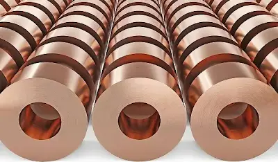
1. Current-Carrying Capability
Copper thickness has a direct relationship with current-carrying capability. For a given trace width and allowable temperature rise, increasing the copper cross-sectional area reduces the current density and allows the trace to carry more current. The source gives a practical example in which 1 oz copper with a 1 mm trace width can carry approximately 1 A. This value should be treated as a design reference for the stated conditions rather than a universal rule, because allowable current also depends on factors such as trace geometry, temperature rise, copper distribution, and cooling conditions.
Power distribution networks, motor drives, battery paths, and other high-current circuits may therefore require 2 oz copper or even copper thicknesses above 10 oz. The appropriate value must be determined from the actual current, trace dimensions, thermal conditions, and manufacturing capability.
2. Thermal Management
Copper is an effective thermal conductor, so increasing copper thickness can improve the ability of a PCB to spread heat away from high-power regions. Thick copper can help distribute heat over a larger area and reduce thermal concentration around high-power conductors and components.
Applications such as high-power LED assemblies and electric-vehicle controllers commonly place significant emphasis on heat dissipation. In these designs, copper thickness is considered together with copper area, thermal vias, component placement, and the board’s overall thermal structure. Copper thickness alone does not determine the complete thermal performance, but it is an important part of the heat-flow path.
3. Controlled Impedance
In high-frequency and high-speed circuits, copper thickness is one of the parameters that affects characteristic impedance. The impedance of a PCB trace is influenced by the trace width, copper thickness, dielectric thickness, dielectric constant, and the relationship between the trace and its reference plane.
For this reason, the impedance calculation must use the finished copper thickness rather than an assumed base copper value. This is particularly important for outer-layer microstrip structures, where the plated copper can change both the physical trace dimensions and the resulting impedance. If the copper thickness used in the stackup calculation does not match the fabricated board, the actual impedance may deviate from the design target.
4. Routing Density and Fine-Line Capability
Copper thickness is generally inversely related to the minimum line width and line spacing that can be manufactured reliably. Thicker copper requires more etching control and makes fine-line formation more difficult because the etchant must remove a greater vertical thickness while limiting lateral undercut.
High-density boards, including HDI boards and smartphone mainboards, may therefore use 0.5 oz or even 1/3 oz ultra-thin copper foil to support fine traces and tight spacing. By contrast, thick-copper boards are better suited to high-current routing and are not normally optimized for very dense interconnects.
This creates a direct design tradeoff. A designer who increases copper thickness to improve current capacity may need to increase line width and spacing, consume more routing area, or accept a less dense layout. A designer who selects thin copper for fine routing must verify that the resulting traces can still meet current and thermal requirements.
5. Cost and Manufacturing Yield
Copper thickness also has a direct effect on PCB cost. Thicker copper foil requires more expensive raw materials, while additional plating increases process time and resource consumption. Thick-copper fabrication can also reduce production yield because etching, lamination, dimensional control, and plating uniformity become more difficult.
For many general-purpose designs, 1 oz copper provides a practical balance among electrical performance, routing density, manufacturability, and cost. It is not automatically the correct choice for every board, but it is often an economical baseline when the application does not require unusually high current, enhanced thermal conduction, or a very fine-line structure.
Balancing Manufacturing Capability and Design Requirements
PCB copper-thickness diversity is the result of a balance between what manufacturing processes can produce reliably and what the circuit requires electrically and thermally. Manufacturing differences between inner and outer layers establish the basic pattern: inner-layer copper is largely determined by the starting foil, while outer-layer copper can be increased through plating.
Design requirements then determine where a particular thickness is appropriate. Current capacity and heat dissipation tend to favor thicker copper. Controlled impedance requires the finished copper thickness to be included in the stackup calculation. High-density routing favors thinner foil, while cost and production yield impose practical limits on both extremes.
As a result, available PCB copper thicknesses range from ultra-thin foil below 0.5 oz to thick copper above 10 oz. The correct choice should not be made from copper weight alone. It should be evaluated against current, thermal performance, impedance, trace geometry, routing density, manufacturing capability, and total cost.