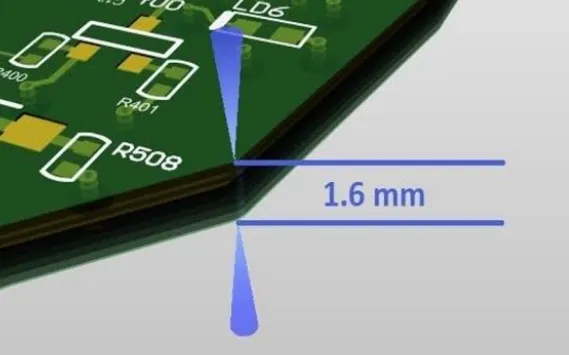
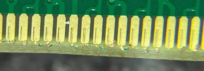
A PCB solder mask may appear to be a thin, secondary coating, but its thickness directly affects solderability, insulation performance, copper protection, and high-speed electrical behavior. A board with an excessively thick solder mask can suffer from poor component coplanarity, solder paste volume variation, blistering, delamination, and impedance deviation. A mask that is too thin may fail to provide adequate insulation, solder mask bridge retention, mechanical protection, or long-term resistance to oxidation and contamination.
The correct target is therefore not simply "as thick as possible." Solder mask thickness must be matched to the PCB structure, component pitch, voltage level, copper thickness, manufacturing process, and reliability requirements.
Why Excessive Solder Mask Thickness Causes Problems
1. BGA Pillow Defects and Reduced Soldering Yield
One of the most easily overlooked problems is the effect of excessive solder mask thickness on component coplanarity. When the mask builds up around a land, it can form a raised boundary around the pad. During placement, the package terminal or solder ball may be lifted slightly above the intended pad surface, preventing complete contact with the printed solder paste.
After reflow, the solder ball and solder paste may appear to be touching, but the connection may not be properly formed. This condition is commonly associated with the BGA "pillow effect," in which the solder ball and the solder paste remain visually adjacent without creating a reliable metallurgical joint.
Reported data indicate that, with conventional copper thickness, the probability of a pillow defect increases by more than 70% when solder mask thickness exceeds 20 μm. For boards with a solder mask thickness above 31.22 μm, direct rejection is generally recommended in the cited case. The effect is particularly significant for bottom-terminated packages such as BGAs and QFNs, where small variations in surface height can directly affect solder joint coplanarity.

2. Uncontrolled Solder Paste Volume
Excessive solder mask thickness can also change the gap between the stencil and the PCB surface. As this gap increases, more solder paste may be deposited during printing. For fine-pitch components with a pitch below 0.4 mm, even a small increase in deposited paste can create a substantial risk of solder bridging and short circuits.
This problem is closely related to the interaction between pad geometry, solder mask height, stencil gasketing, and paste release. A solder mask that is too high can prevent the stencil from sealing properly against the board. The result is not only a change in paste volume but also greater variation from pad to pad, which can make the subsequent reflow process less tolerant of printing deviations.
3. Reduced Adhesion, Blistering, and Delamination
When solder mask ink is applied too thickly, solvents and trapped air within the coating may not be fully removed during pre-baking. After curing, residual voids or solvent pockets can remain inside the film. During the high-temperature exposure of reflow or wave soldering, these inclusions may expand rapidly, causing the solder mask to blister or detach over a larger area.
The risk is more pronounced on heavy-copper boards. Thick copper traces create larger steps between the copper surface and the laminate. Solder mask tends to accumulate at these step transitions, producing a locally excessive film thickness. After curing, the coating may experience increased mechanical stress and separate from the copper surface, especially near sharp transitions or poorly covered sidewalls.
4. Impedance Deviation in High-Frequency Circuits
Solder mask also affects the electrical environment around a PCB trace. Its dielectric constant, approximately 3.2 to 4.0 in the cited range, is higher than that of air. When the mask covers a trace, it increases the effective dielectric loading around the conductor and generally lowers the trace impedance.
For the stated design case, every additional 10 μm of solder mask thickness reduces impedance by approximately 1 to 2 Ω. In high-speed differential designs, this deviation can affect differential impedance, mode conversion, insertion loss, and overall signal integrity. The impact depends on the trace geometry, reference-plane spacing, dielectric properties, and whether the trace is covered by solder mask on one or both sides.
For this reason, solder mask thickness should not be treated as an isolated cosmetic parameter in high-speed designs. It may need to be included in the impedance calculation and verified against the actual fabrication stackup.
5. Solder Mask Bridges Are Not Always Stronger When Thicker
A solder mask bridge between fine-pitch pads must satisfy a delicate relationship between width, height, exposure, and curing conditions. If the bridge is too thick but too narrow, the uncured material may be washed away during development. Even if the bridge remains after development, it may lift or delaminate under thermal stress during soldering.
Therefore, increasing solder mask thickness does not automatically improve bridge reliability. A narrow bridge needs sufficient exposure and adhesion throughout its cross-section, while excessive height can increase the mechanical stress generated during thermal cycling.

Risks Associated with Insufficient Solder Mask Thickness
1. Reduced Electrical Insulation
The DC dielectric strength of the solder mask is approximately 20 kV/mm in the cited example. At a thickness of 10 μm, the theoretical withstand voltage is approximately 200 V. In high-voltage areas, such as electric-vehicle control boards and power modules, insufficient coating thickness directly increases the risk of insulation breakdown.
High-voltage boards commonly specify a solder mask thickness of at least 30 μm for this reason. However, the required thickness should still be determined together with clearance, creepage distance, contamination conditions, voltage category, and the applicable product requirements. A thicker coating cannot compensate for inadequate spacing or poor surface cleanliness.
2. Solder Mask Bridges May Be Washed Away or Delaminate
If a solder mask bridge is too thin, the uncured material may not polymerize adequately through its full thickness. During alkaline development, the bridge can be partially or completely removed. Even when it survives development, a thin film may have insufficient adhesion to the substrate and copper surface.
During reflow at temperatures above 260 °C, thermal stress can cause the thin bridge to lift or delaminate. Molten solder may then spread between adjacent pads, creating a short circuit. This risk is especially serious for fine-pitch components, where the remaining gap between pads is small and even minor mask damage can affect solder containment.
3. Loss of Copper-Surface Protection
The primary function of solder mask is to isolate exposed copper from air, moisture, and chemical contaminants. When the coating thickness falls below 8 μm, the risk of copper oxidation increases sharply. Moisture and corrosive substances can penetrate the film more easily, reducing long-term reliability.
Thin or locally incomplete coverage can also create areas that resemble exposed copper. These areas may not always represent a complete coating failure, but they can still weaken corrosion resistance and may be rejected under strict appearance or reliability criteria.
4. Inadequate Mechanical Protection
A thin solder mask generally has lower resistance to scratching and abrasion. During assembly, handling, transportation, and service, the coating may be damaged by contact with tools, fixtures, or adjacent hardware. Once the copper conductor is exposed, corrosion can begin at the damaged area and gradually spread along the surface.
Mechanical protection is particularly important around exposed routing, connector areas, and regions that may experience repeated handling. A uniform coating is more reliable than a nominal thickness that is achieved only in isolated areas.
What Solder Mask Thickness Is Appropriate?
Different applications require different thickness targets. The following values are industry reference ranges from the cited design context and should not be treated as universal acceptance limits.
- General consumer electronics: 10–25 μm, balancing cost, manufacturability, and reliability.
- Fine-pitch BGA applications: 15 ± 5 μm, with emphasis on solder-ball coplanarity and printing consistency.
- High-voltage power boards: ≥30 μm, with emphasis on insulation performance.
- Military and automotive electronics: 25–35 μm, with emphasis on environmental durability.
In many cases, the thickness tolerance should be controlled within ±5 μm. The required value should be clearly specified in the fabrication documentation or fabrication drawing rather than left to interpretation. Where solder mask thickness affects soldering, insulation, or impedance, the requirement should be reviewed together by the PCB designer, manufacturer, and assembly engineer.
Key Process Controls for Solder Mask Thickness
1. Select the Coating Method According to the Application
Screen printing has a relatively low cost but generally provides lower thickness uniformity. Curtain coating can provide better overall uniformity, while spray coating is suitable for boards with heavy copper and significant surface-height variation.
Dry-film solder mask can achieve thickness uniformity of approximately ±2 μm, compared with approximately ±5 μm for liquid photoimageable solder mask, or LPI. However, dry-film processes generally involve higher cost. The selection should therefore consider not only the nominal thickness but also pad density, copper topography, bridge requirements, and production volume.
2. Match Pre-Baking and Exposure to the Coating Thickness
The thicker the ink film, the more carefully the pre-bake time must be controlled. If the pre-bake is insufficient, solvents may remain inside the coating and later produce voids, blistering, or adhesion problems during thermal processing.
Exposure energy must also be adjusted according to the coating thickness. Excessive thickness combined with insufficient exposure can leave the lower portion of the film under-cured. During development, this may lead to undercutting, sidewall erosion, or loss of narrow solder mask bridges.
3. Control Copper Thickness Uniformity
Solder mask uniformity depends significantly on the uniformity of the copper surface beneath it. When copper thickness varies, the surface topography changes, and the coating naturally becomes thicker in some locations and thinner in others. This is an important root cause that can be overlooked when only the solder mask process is investigated.
Heavy-copper transitions, trace edges, pads, and other abrupt height changes should receive particular attention. A stable copper-plating process and appropriate design of copper features help reduce local solder mask accumulation.
4. Verify Thickness with Cross-Section Analysis
Metallographic cross-section analysis remains a key method for verifying solder mask thickness. A properly prepared cross-section can reveal the coating thickness, profile, coverage over copper steps, adhesion condition, and defects such as voids or delamination.
Eddy-current thickness measurement can also be used for production monitoring, but measurement methods should be selected according to the board construction and the capability of the equipment. For critical products, cross-section verification provides more complete information because it shows not only thickness but also the actual shape and condition of the coating.
Finding the Balance Between Protection and Manufacturability
Solder mask thickness is fundamentally a balance between excessive coating and insufficient protection. A coating that is too thick may reduce soldering yield, produce blistering or delamination, alter controlled impedance, and compromise fine-pitch solder mask bridges. A coating that is too thin may provide inadequate insulation, fail to contain molten solder, expose copper to the environment, and offer poor resistance to mechanical damage.
There is no single thickness suitable for every PCB. The appropriate target must be matched to the component pitch, copper thickness, voltage level, high-speed requirements, coating process, and end-use environment. Clear fabrication documentation, control of the underlying copper topography, correct pre-bake and exposure settings, and verification through cross-section analysis are all necessary to achieve a stable result.