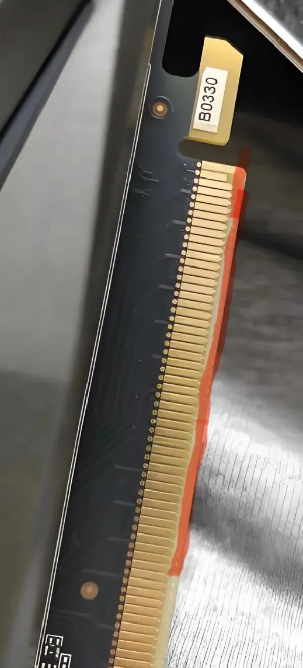
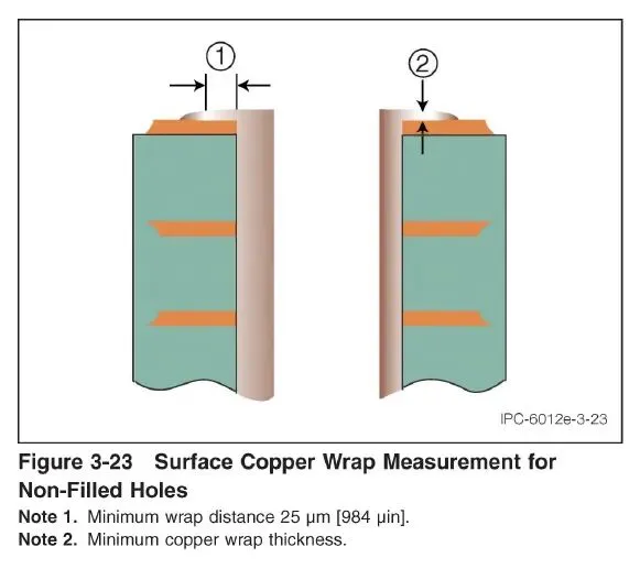
Many layout engineers select via tenting or via exposure almost automatically. However, once the board reaches electrical testing, reflow soldering, wave soldering, or assembly beneath a BGA, that choice is no longer a matter of drafting preference. It can directly affect manufacturing quality and product reliability.
Tenting, Plugging, and Via Filling Are Not the Same
A common misconception must be corrected first: a tented via is not the same as a plugged via, and neither is the same as a filled and capped via.
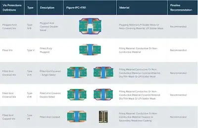
- Via tenting: solder mask covers the via opening, while the hole itself remains empty. The primary purposes are to prevent solder from adhering to the via and to provide basic electrical insulation.
- Via plugging: ink or resin is used to close the hole so that solder cannot readily flow through it.
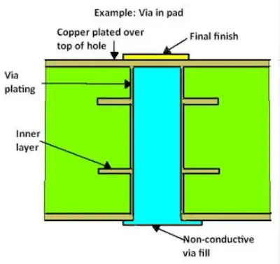
- Via filling and capping: resin completely fills the via, the surface is planarized, and copper is plated over the filled hole. The finished surface is approximately level with the surrounding pad. This is the structure typically required for via-in-pad applications under a BGA.
In terminology associated with IPC-4761 protection types, these structures correspond broadly to Type I for tenting, Types III and IV for plugging, and Type VII for filling and capping.
Choose the Via Finish According to Its Function
Instead of asking only whether a via should be exposed or tented, first determine what the via must do. Does it need to be completely filled? Must it be solderable? Does a test probe need to contact it?
When Via Tenting Is the Normal Choice
For most ordinary signal vias and power vias that are not used for testing, thermal transfer, or via-in-pad assembly, tenting is a conventional and economical choice.
However, via diameter must be considered. For a tented via, the hole diameter is preferably controlled to 0.4 mm or less and should generally not exceed 0.5 mm. Once the diameter exceeds 0.5 mm, solder mask becomes less capable of reliably covering the annular ring. In such cases, the PCB fabricator may not accept responsibility for incomplete tenting or exposed areas around the opening.
A tented via may also show a yellowish appearance around the opening. This does not necessarily indicate a manufacturing defect. During curing, liquid solder mask can flow partially into the hole, making the mask thinner around the annular ring and allowing the copper color to show through. This is an inherent characteristic of the tenting process.
The key limitation is that tenting seals the opening; it does not fill or block the hole. During wave soldering or selective soldering, the hole remains empty, so solder may still pass through it. Tenting alone is therefore insufficient when solder penetration must be prevented.
Three Situations That Require Via Exposure
1. ICT or FCT Probe Access
Because solder mask is electrically insulating, a test probe cannot make reliable electrical contact with a tented via. A via used for in-circuit testing or functional testing must therefore be exposed on the probe side so that the probe can contact the copper surface.
There is an important caveat: do not simply expose an unfilled via without considering probe stability. The probe tip may drop into the hole, resulting in inconsistent contact and possible damage to the test fixture. A more reliable structure is to plug or fill the via first and then expose the conductive surface. A filled, planarized contact area provides a more stable target for the probe.
2. Parallel Vias in a High-Current Path
When a single via cannot carry the required current, multiple vias may be connected in parallel. For example, a 0.3 mm via with 25 μm hole-wall copper, good heat dissipation through the outer layer, and a 10 °C temperature rise can carry approximately 1 A under the stated conditions. A current approaching 2 A depends strongly on the thermal environment and construction details. Using one via for 3 A or 5 A is generally inappropriate in this type of design.
With an exposed via, solder deposited during reflow can cover the annular ring and potentially increase the effective conductive and thermal cross-sectional area. However, this benefit depends on solder actually entering and remaining around the via. Exposure alone does not automatically increase current capacity. The improvement must be evaluated together with the soldering process, via geometry, copper thickness, and thermal conditions.
3. Via Arrays Beneath Thermal Pads
Via arrays placed beneath thermal pads are used to transfer heat into internal or opposite-side copper structures. Solder mask adds thermal resistance, whereas an exposed copper surface can make direct contact with air or a thermal interface and become part of the heat-transfer path.
Exposing vias also introduces disadvantages. Bare copper can oxidize, and adjacent exposed vias or pads may bridge during HASL processing if their spacing is too small.
A commonly applied minimum condition is a spacing of at least 0.2 mm from the edge of the via pad to the edge of the adjacent pad. If the layout cannot maintain this clearance, an ENIG surface finish may reduce the risk of solder bridging compared with HASL. The actual manufacturability limit should still be confirmed with the fabricator.
Via-in-Pad Requires Filling and Capping
When a via is placed directly in a component pad, particularly beneath a BGA, neither ordinary tenting nor simple exposure is sufficient.
An unfilled via-in-pad can draw molten solder down along the hole wall during reflow. This phenomenon, known as solder wicking, can leave the BGA joint with insufficient solder or create voids and incomplete connections. The result may be an unreliable solder joint or an intermittent BGA connection.
For this reason, a via-in-pad structure generally requires resin filling, surface grinding or planarization, and copper plating over the filled via. This is the filled-and-capped structure identified as IPC-4761 Type VII.
Ink plugging is not an equivalent substitute for resin filling in a BGA pad. Ink can crack or form bubbles during thermal cycling, and the resulting surface may not be sufficiently flat for reliable BGA assembly. A via located on a component pad should therefore be filled with resin or copper paste as required by the selected fabrication process, rather than merely plugged with solder mask ink.
Thermal design must also be considered for filled vias in BGA corner regions. If the filled via is not connected to a sufficiently large internal copper area, rapid cooling during reflow can contribute to cold-tear or shrinkage-related cracking and solder-joint damage. The via structure, copper connection, pad geometry, and thermal behavior should be reviewed together instead of treating the via finish as an isolated setting.
Make the Fabrication Documentation Explicit
If tenting is selected in the design data, the solder-mask layer in the Gerber output must reflect that decision consistently. For via-in-pad structures, simply drawing the via inside the pad is not enough. The fabrication notes should explicitly specify the required construction, for example: "IPC-4761 Type VII, resin-filled and copper-capped."
Without a clear note, a fabricator may process the feature as a standard tented via or an ordinary plugged via according to its default interpretation. That difference can determine whether the BGA assembly is reliable or fails because of solder wicking and insufficient solder volume.
The correct choice depends on the electrical, thermal, testing, and assembly functions of the via. Tenting is suitable for many ordinary vias, exposure is necessary where probe contact or solder-assisted conduction is required, and via-in-pad applications normally require a properly filled and capped structure.