Adding Fiducial Marks to a Narrow Rigid-Flex PCB
During CAM review of a 6-layer rigid-flex order measuring 205 × 20 mm with a finished board thickness of 1.6 mm, immersion gold surface finish of 1.00 µm, and customer-requested panelization (1 × 5 with 4 mm process edges in four directions), the engineering team received an explicit instruction to add MARK points. The specified parameters were a mark size of 1.0 mm, a solder-mask window of 1.4 mm, identical XY location on the top and bottom layers, and copper cleared on the bottom layer. The production artwork was to be confirmed after implementation. Quantity is 125 pcs (25 sets), area approximately 0.5751 m², via treatment is cover-oil, minimum hole diameter 0.3 mm, line width/spacing 6 mil, no impedance control, flying-probe full test, IPC-II acceptance criteria, and forming by routing slots plus laser. The flexible sections are 2-layer, 0.1 mm thick, Shengyi SF305C with yellow solder mask and white silkscreen, copper 1/3 oz both sides, no reinforcement or adhesive. The rigid sections use FR-4 Shengyi S1150G (TG155), green solder mask top and bottom, white silkscreen, and 1 oz copper. These parameters define the practical boundaries for implementing the fiducials without conflicting with the existing panelization scheme, the mixed rigid-flex process, or the cover-oil via treatment.
The request arrived as a fabrication requirement rather than a correction of already-present features. This indicates that the original design data either omitted fiducials entirely or left their dimensions, openings, and copper clearances unspecified. From a manufacturing perspective, the critical consideration was therefore to realize the stated geometry in the production artwork while preserving the integrity of the copper, solder-mask, and immersion-gold layers and remaining compatible with the 1 × 5 panel layout and the subsequent laser-assisted forming.
Fiducial Mark Size, Solder Mask Clearance, and Copper Spacing
Fiducial marks provide the optical reference that automated assembly equipment uses to locate a board or panel. A 1.0 mm copper feature with a 1.4 mm solder-mask opening produces a 0.2 mm annular clearance around the mark. This clearance is relatively tight for immersion-gold processing. Any residual solder-mask bleed, incomplete mask development, or gold-plating edge effects that encroach on the 1.0 mm copper area can reduce the contrast available to typical vision systems under standard lighting. Because the order specifies immersion gold rather than HASL or OSP, the plated surface must remain free of nodules or thickness variation that would alter the optical signature of the 1.0 mm feature.

The requirement that the top and bottom marks occupy the identical XY location, with bottom copper hollowed out, adds a second constraint. Clearing the bottom copper prevents an opposing copper feature from creating a double image or from interfering with through-board recognition if the assembly process uses dual-side cameras or if light transmission through the board is relevant. On a rigid-flex construction the rigid portions are the only practical locations for reliable fiducials; the 0.1 mm flexible sections lack the dimensional stability needed for optical targets. The 4 mm process edges on the 1 × 5 panel therefore become the natural candidate areas, provided the marks do not encroach on the routing-slot separation paths or the laser contour zones.
The narrow 20 mm board width further restricts placement. Marks located too close to the long edges risk being affected by process-edge compensation or by the final laser contour. Because the order ( #RFP-20260708-046 ) accepts cross boards and outsourced fabrication under IPC-II criteria, the CAM engineer must ensure that the added features remain within the agreed design intent and do not introduce process deviations that would require additional re-confirmation. The mixed solder-mask colors—green on the rigid sections and yellow on the flexible sections—also affect local contrast; a fiducial placed near a rigid-flex transition must be evaluated for possible mask-color boundary effects on optical recognition, even though the primary target areas remain the rigid process edges.
CAM Review of Fiducial Placement and Copper Clearance
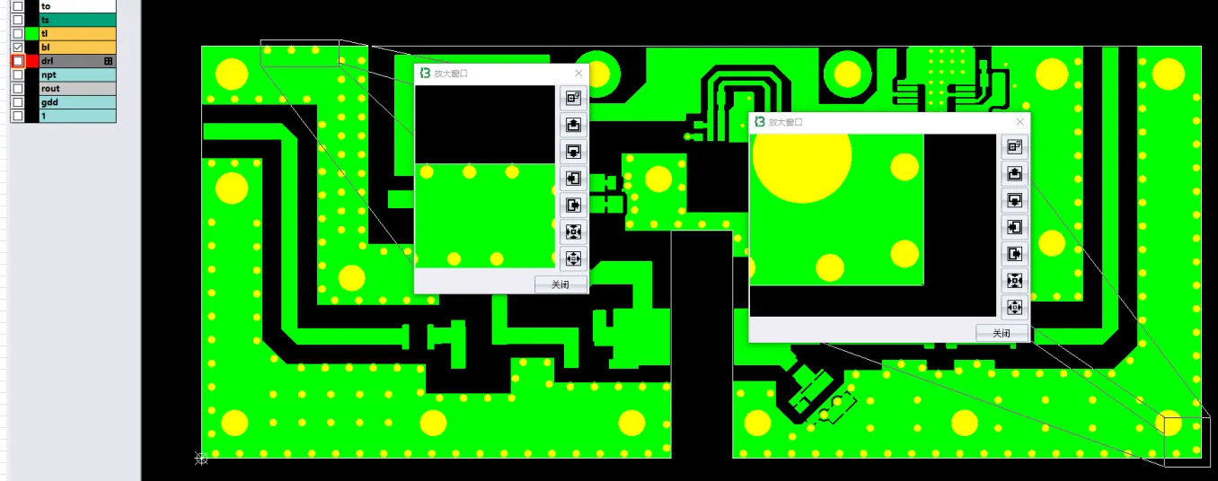
Implementing the marks requires coordinated changes across copper, solder-mask, and drill or outline layers while maintaining the existing 6 mil design rules and cover-oil via treatment. The 1.0 mm copper pads must be added with the precise 1.4 mm mask openings; any misalignment between copper and mask data can leave part of the copper covered or create an oversized opening that reduces the effective contrast annulus. On the bottom layer the copper must be cleared at the same XY coordinate so that no residual copper remains under the top-side mark. Because the panel is 1 × 5 with 4 mm process edges, the marks are most appropriately located within those process edges rather than on the individual 205 × 20 mm units. Placement must still clear the routing-slot paths used for separation and the laser-assisted forming zones so that the fiducials survive panel separation and remain available for assembly.

The immersion-gold process adds a further check. Gold plating thickness of 1.00 µm must be uniform across the 1.0 mm feature; edge effects or plating-tank current-density variations near the process-edge copper can alter the optical reflectivity. The cover-oil via treatment does not directly affect the fiducials provided the marks are kept clear of any vias, yet the overall panel copper balance must be reviewed so that the added pads do not create local density changes that influence plating uniformity. After the marks are inserted, the revised production artwork (Gerber or ODB++) must be verified for absence of unintended shorts, mask bridges, or plating anomalies, particularly near the process edges where the panel is later separated by routing slots plus laser.
The rigid-flex PCB stack-up itself imposes material constraints. The flexible sections use 1/3 oz copper on Shengyi SF305C, while the rigid sections use 1 oz copper on S1150G (TG155). Fiducials placed on the rigid portions therefore sit on the thicker copper and the more dimensionally stable FR-4. Any fiducial that approaches a rigid-flex transition must be checked for registration between the rigid and flex layers so that the 1.0 mm copper feature and its 1.4 mm opening remain concentric after lamination and cover-layer application. Because the order specifies no reinforcement on the flex and no electromagnetic film, the transition zones remain relatively thin; marks placed too close to these zones risk dimensional shift during the laser contouring step.
Interaction with Panelization, Forming, and Confirmation Workflow
The 1 × 5 panelization with 4 mm process edges and zero-gap routing-slot spacing means the individual boards are closely nested. Fiducials added in the process edges must remain outside the final laser contour and the routing-slot paths so that they are not removed during separation. The forming method therefore defines a keep-out zone around each mark. Because the production artwork must be confirmed, the CAM engineer prepares the revised data, documents the exact XY locations chosen within the process edges, and returns the files for customer review. This confirmation step is essential: once the marks are present, any subsequent change to location or geometry would require re-generation of the copper and mask layers and re-verification against the cover-oil and immersion-gold processes.
Other order parameters—flying-probe full test, electronic delivery of electrical-performance and quality reports, 24-day lead time—do not alter the fiducial geometry, yet they reinforce the need for a clean, confirmable artwork revision. Automated optical inspection of the finished panel will treat the fiducials as non-functional copper features; their geometry must therefore be stable enough not to generate false defects. Leaving the dimensions, the matched top/bottom location, or the bottom copper clearance undefined would have transferred the interpretation risk downstream, either to a fabricator default library or to the assembler. In that case the resulting marks could be too small for reliable vision, partially covered by solder mask, or opposed by residual copper that reduces optical contrast—each of which is a potential assembly-alignment risk rather than a confirmed defect in the present order.
Verifying Fiducial Locations Before Rigid-Flex PCB Production
Our engineering team treated the instruction as a controlled fabrication requirement equivalent to any other copper or mask geometry. The combination of a long, narrow rigid-flex outline, 1 × 5 panelization with defined process edges, immersion gold, mixed solder-mask colors, and laser-assisted forming made the confirmation step non-negotiable. Implementing the 1.0 mm marks with 1.4 mm openings, identical top/bottom location, and bottom copper clearance, then verifying clearance to all adjacent process features, keeps the optical targets aligned with the stated design intent while respecting the physical constraints of the rigid-flex stack-up and the chosen panelization method.
The practical lesson from this order is that when a customer supplies explicit fiducial size, opening, and copper-clearance values, the CAM workflow should implement those values, document the chosen locations within the process edges, check concentricity and contrast against the immersion-gold and mixed-mask processes, and return the revised production draft for confirmation before release. Doing so prevents the optical targets from becoming an interpretation item later in fabrication or assembly and maintains consistency with the IPC-II acceptance criteria already agreed for the order. The same discipline applies to any subsequent revision: once the marks are locked in the confirmed artwork, further changes must again pass through the same geometric and process verification steps.