Introduction
High-speed PCB manufacturing demands a delicate balance between achieving superior signal integrity and controlling costs. As electronic devices operate at frequencies exceeding several gigahertz, engineers face challenges like signal loss, crosstalk, and impedance mismatches that can degrade performance. Yet, escalating material and process expenses often strain project budgets. This article explores proven strategies to optimize high-speed PCB cost without sacrificing reliability. Factory-driven insights reveal how thoughtful decisions in material selection, layer count, via types, and design complexity can yield substantial savings. By adhering to established standards, manufacturers ensure quality while minimizing PCB fabrication cost.
Why High-Speed PCBs Drive Up Manufacturing Costs
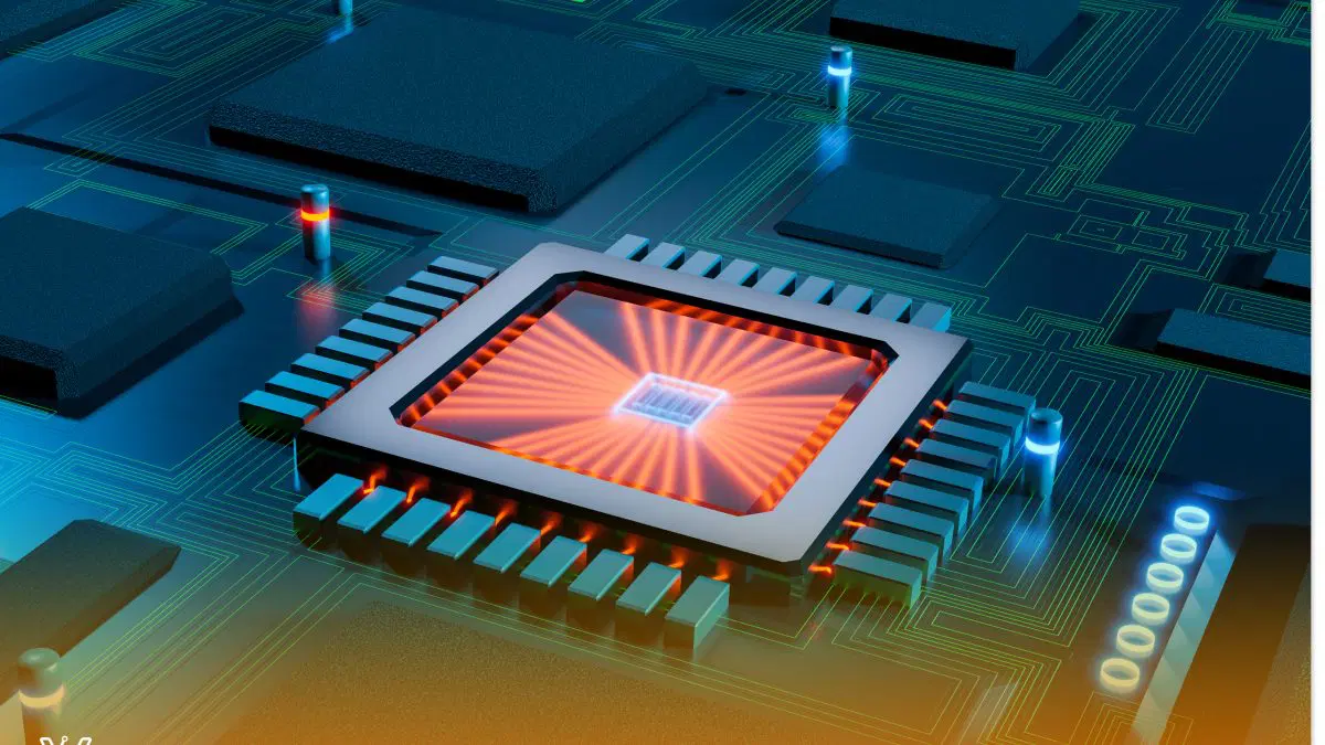
High-speed PCBs support data rates from 10 Gbps upward, requiring precise control over electrical characteristics. Conventional FR-4 materials suffice for lower speeds, but higher frequencies necessitate low-loss dielectrics to reduce attenuation and maintain signal fidelity. Increased layer counts accommodate dense routing and shielding, yet each additional layer adds to lamination, drilling, and plating expenses. Complex via structures, such as blind or buried types, enhance performance by shortening signal paths but introduce sequential build processes that inflate high-speed PCB cost. Design complexity, including fine-pitch traces and controlled impedance, demands advanced imaging and etching, further elevating fabrication expenses. Understanding these drivers enables engineers to target cost reductions effectively.
Key Factors Influencing High-Speed PCB Cost
Material Selection Impacts
Material selection profoundly affects both performance and high-speed PCB cost. Dielectrics with low dielectric constant (Dk) and dissipation factor (Df) minimize signal propagation delays and losses, essential for high-frequency operation. Standard FR-4 offers cost advantages but exhibits higher Df at gigahertz ranges, leading to unacceptable insertion loss in demanding applications. Low-loss variants or specialized resins provide better performance yet command premium pricing due to raw material scarcity and processing challenges. Factory experience shows that hybrid stackups, combining standard cores with low-loss skins, balance these trade-offs. Proper selection aligns with IPC-6012F qualification requirements for rigid printed boards, ensuring mechanical stability alongside electrical performance.
Layer Count and Stackup Optimization
Layer count directly correlates with PCB fabrication cost, as multilayer boards involve more lamination cycles and alignment precision. High-speed designs often require 8 to 16 layers for power planes, ground shielding, and differential pairs to mitigate EMI. Excessive layers increase material usage and yield risks from warpage or delamination. Optimized stackups group signal layers adjacent to reference planes, reducing crosstalk without extra layers. Engineers can simulate stackups to verify impedance control, avoiding over-design. Reducing from 12 to 10 layers, for instance, can cut costs by streamlining via transitions and build sequences.
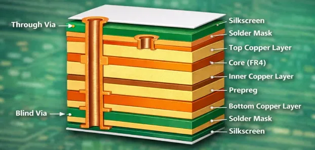
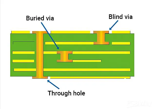
Via Types and Their Cost Implications
Via types play a critical role in high-speed signal routing and manufacturing economics. Through-hole vias are simplest and cheapest, spanning all layers but creating stubs that cause reflections at high frequencies. Blind and buried vias connect specific layers, eliminating stubs for cleaner signals, though they require laser drilling or sequential lamination, raising costs. Microvias enable higher density in HDI boards, vital for compact high-speed layouts, but their small aspect ratios demand precise control to avoid reliability issues like cracking. Strategic use of via types, per IPC-2221G design guidelines, minimizes total via count while preserving performance. Factories prioritize via farms or stitching only where EMI suppression necessitates them.
Design Complexity and Prototyping Expenses
Design complexity amplifies high-speed PCB cost through tighter tolerances and inspection needs. Fine-line traces below 4 mils and spaces demand LDI exposure for accuracy, increasing setup times. Controlled impedance requires consistent dielectric thickness, complicating panelization. Prototyping iterations expose these issues early, but multiple spins erode budgets. Streamlined designs with wider tolerances where possible reduce high-speed PCB cost. Early DFM reviews catch over-specifications, aligning with fabrication capabilities.
Practical Strategies for Cost Reduction in High-Speed PCB Manufacturing
Smart Material Selection for Balanced Performance
Prioritize materials based on frequency needs rather than blanket upgrades. For signals up to 25 Gbps, enhanced FR-4 with Df below 0.01 suffices, avoiding exotic laminates reserved for 56 Gbps plus. Evaluate total stackup loss budgets via simulations before specifying. Hybrid constructions use cost-effective cores for inner layers and low-loss outer skins for critical traces. This approach cuts material expenses by 20-30% in many designs while meeting IPC-A-600K acceptability criteria. Factories recommend qualifying materials through thermal cycling to ensure long-term reliability.
Minimizing Layer Count Through Efficient Routing
Achieve high-speed performance with fewer layers by leveraging broadside coupled striplines and embedded components. Pair high-speed nets on inner layers flanked by planes for inherent shielding. Backdrilling through-vias removes stubs affordably compared to blind vias. Advanced routing algorithms optimize trace lengths, reducing the need for extra layers. A 6-layer board can handle many 10 Gbps applications if stackup symmetry prevents warpage. This strategy lowers lamination costs and improves yields.
Optimizing Via Usage and Types
Limit blind and microvias to critical high-speed nets, using through-vias elsewhere. Convert unnecessary microvias to larger laser vias for cost savings in drilling. Via-in-pad designs increase density but require filled vias to avoid solder wicking issues. Factories favor staggered via sequencing to simplify build-ups. Per design standards, cap via counts per net to essential fanouts. These tactics reduce sequential processes, slashing high-speed PCB cost.
Simplifying Design Complexity
Standardize trace widths and spaces across nets to minimize retooling. Use symmetric stackups for natural impedance matching. Incorporate test points judiciously to cut probing expenses. Panelize designs efficiently for volume runs. Prototyping focuses on small panels first, validating signal integrity before full production. This iterative approach controls PCB fabrication cost.
Prototyping and Manufacturing Best Practices
Prototype with relaxed tolerances initially, tightening only after validation. Leverage quick-turn fabs for 4-8 layer proofs-of-concept. Volume manufacturing benefits from large panels and standard thicknesses. Implement statistical process control for consistent yields. Adhering to IPC standards during fabrication ensures first-pass success, avoiding costly respins.
Real-World Insights from Factory Production
In production runs for networking gear, switching from all-blind vias to hybrid through/blind configurations saved 15% on fabrication while maintaining 40 Gbps integrity. Another case involved downgrading non-critical layers to standard FR-4, redirecting budget to low-Df signal layers. These adjustments followed IPC-6012F performance specs, yielding robust boards. Engineers report that pre-production DFM audits prevent 80% of cost overruns. Such factory-driven tweaks prove essential for high-speed PCB manufacturing.
Conclusion
Cost-effective high-speed PCB manufacturing hinges on informed choices in material selection, layer count, via types, design complexity, and prototyping. By optimizing these elements, engineers balance stringent performance needs with budget constraints. Factory insights underscore the value of standards compliance for reliability. Implementing these strategies reduces high-speed PCB cost significantly, enabling competitive designs. Procurement teams gain leverage through precise quoting based on simplified specs. Ultimately, these practices drive innovation without financial compromise.
FAQs
Q1: How does material selection affect high-speed PCB cost in manufacturing?
A1: Material selection directly influences high-speed PCB cost due to varying dielectric properties and processing demands. Low-loss materials enhance signal integrity at high frequencies but increase raw material expenses. Standard FR-4 suits moderate speeds cost-effectively, while hybrids optimize budgets. Factories advise simulating loss budgets to justify premiums. Compliance with IPC-6012F ensures performance without excess spending.
Q2: What role does layer count play in PCB fabrication cost for high-speed designs?
A2: Layer count escalates PCB fabrication cost through added lamination and alignment steps. High-speed boards need multiple planes for shielding, but optimization reduces this to essentials. Symmetric stackups minimize warpage risks and expenses. Simulations verify fewer layers suffice for impedance control. Factory best practices cut costs by 10-20% via efficient routing.
Q3: How can via types help reduce high-speed PCB cost?
A3: Via types impact high-speed PCB cost via drilling and build complexity. Through-vias are cheapest but stub-prone; blind and buried vias improve signals at higher cost. Limit advanced vias to critical nets, using backdrilling for affordability. IPC-2221G guides strategic placement. This balances performance and manufacturing economics effectively.
Q4: What prototyping strategies lower overall high-speed PCB manufacturing expenses?
A4: Prototyping strategies curb high-speed PCB manufacturing expenses by validating designs early. Start with small panels and standard processes, iterating based on signal tests. DFM reviews simplify specs pre-production. Quick-turn fabs accelerate feedback without full costs. Standards adherence prevents respins, optimizing total spend.
References
IPC-6012F — Qualification and Performance Specification for Rigid Printed Boards. IPC, 2023
IPC-2221G — Generic Standard on Printed Board Design. IPC, 2017
IPC-A-600K — Acceptability of Printed Boards. IPC, 2020


