










PCB Specifications
| Parameter | Value | Parameter | Value |
|---|---|---|---|
| PCB Type | FR4 PCB | Quantity | 30 pcs |
| Layers | 10 Layers | Board Type | Panel PCB |
| Dimensions | 324.8 x 76.8 mm | Copper Weight | 1oz |
| Thickness | 1.6 mm | Min Track / Spacing | 6/6mil↑ |
| Surface Finish | ENIG (Immersion Gold) | Min Hole Size | 0.3mm↑ |
| Solder Mask | Green | Silkscreen | White |
| Stack-up | Custom | Impedance Control | Yes |
| Blind/Buried Vias | No |
Manufacturing Timeline
Logistics Information
Key Manufacturing Processes
Manufacturing Summary
This 10-layer FR-4 PCB measured 324.8 × 76.8 mm with 1.6 mm thickness, TG170 material, and asymmetric copper of 0.5 oz inner / 1 oz outer. Produced as 30 pieces in 1×2 panels for 15 sets, the order used ENIG surface finish (1 µin gold), green solder mask, and white silkscreen. The design included controlled impedance, resin-plugged vias, gold fingers with bevel, and 0.3 mm minimum holes at standard 6 mil line/space. Process edges of 4 mm on the left and right sides supported V-cut separation. The 20-day schedule included 100% flying probe testing.
DFM review focused on stackup, impedance, and production-file alignment. The supplied production draft was confirmed as the manufacturing reference. Customer stackup and impedance requirements were adjusted slightly to match available materials while preserving overall targets. Differential impedance line spacing in the notes did not match the actual Gerber data, and several impedance lines referenced layers that did not exist in the stackup; control was limited to the traces that could be clearly identified and compensated.
Confirmed stackup revision, impedance scope, and file alignment were implemented prior to production. The long multilayer boards achieved consistent ENIG plating, reliable resin filling, and controlled impedance performance within the planned timeline. Full electrical test reports and quality certificates accompanied the shipment, confirming the panels met the specified mechanical and electrical requirements.
Explore More PCB Manufacturing Resources
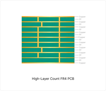
High-Layer Count FR4 PCB Manufacturing
These high-layer count FR4 PCB enable high-density interconnects while maintaining signal integrity and thermal reliability in computing and communication equipment.
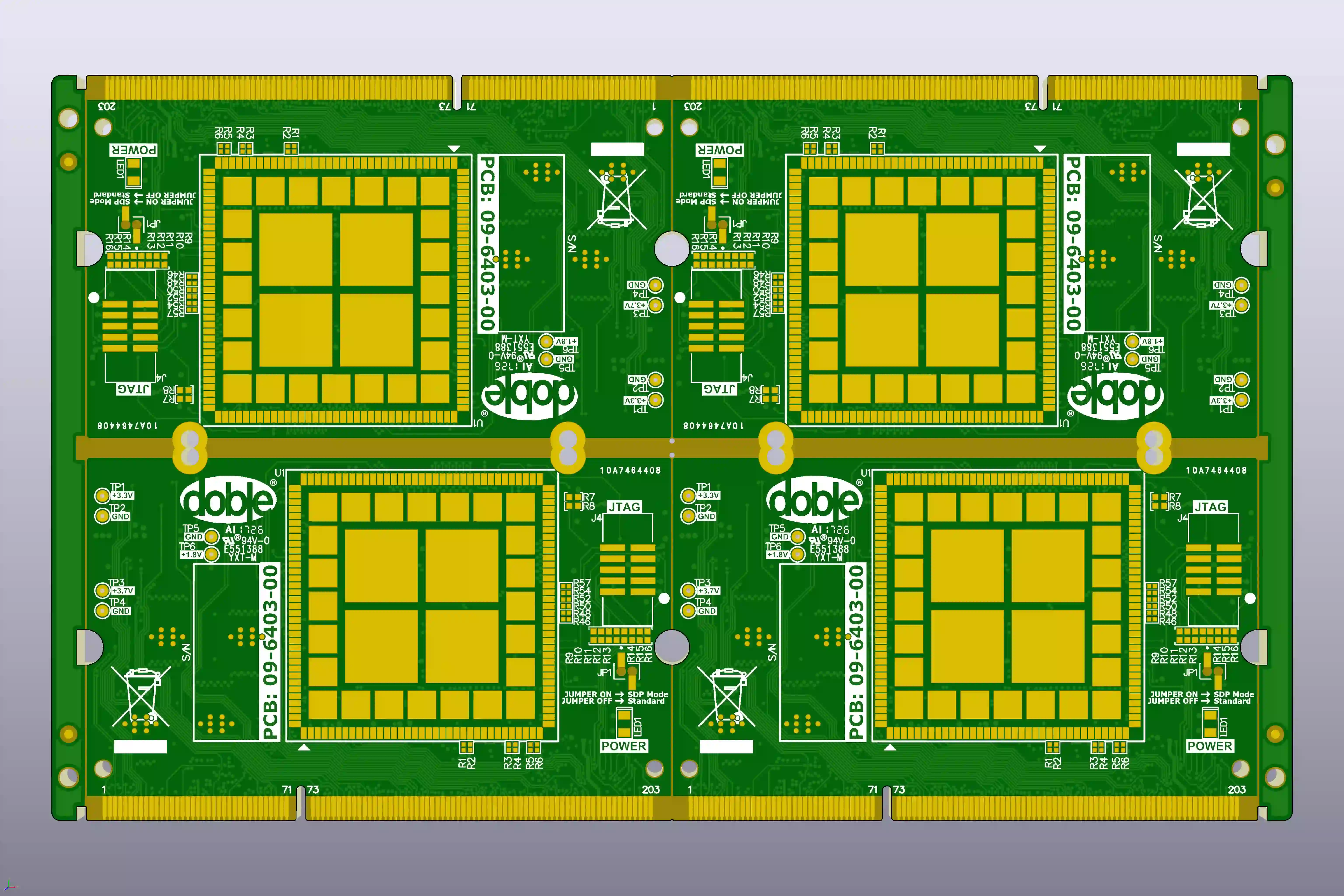
How to Resolve Gold Finger Bevel and Impedance EQs in 10-Layer PCBs
Real 10-layer FR-4 case study: how CAM engineers resolved gold finger bevel clearance, impedance mismatch, tight via spacing and plugging risks to prevent scrap and signal integrity failures.
Real Production Records
| Order ID | PCB Type | Layers | Dimensions | Solder Mask | Surface Finish | Quantity | Action |
|---|---|---|---|---|---|---|---|
| FR4-20260918-033 | FR4 PCB | 6 | 55 x 41.7 | Green | ENIG (Immersion Gold) | 5 | View detail |
| FR4-20260912-059 | FR4 PCB | 2 | 275 x 193.7 | Green | ENIG (Immersion Gold) | 100 | View detail |
| FR4-20260819-043 | FR4 PCB | 10 | 157 x 140 | Blue | ENIG (Immersion Gold) | 100 | View detail |


