










PCB Specifications
| Parameter | Value | Parameter | Value |
|---|---|---|---|
| PCB Type | FR4 PCB | Quantity | 10 pcs |
| Layers | 12 Layers | Board Type | Panel PCB |
| Dimensions | 235.13 x 259.7 mm | Copper Weight | 1oz |
| Thickness | 2 mm | Min Track / Spacing | 6/6mil↑ |
| Surface Finish | ENIG (Immersion Gold) | Min Hole Size | 0.3mm↑ |
| Solder Mask | Red | Silkscreen | White |
| Stack-up | Custom | Impedance Control | Yes |
Manufacturing Timeline
Logistics Information
Key Manufacturing Processes
Manufacturing Summary
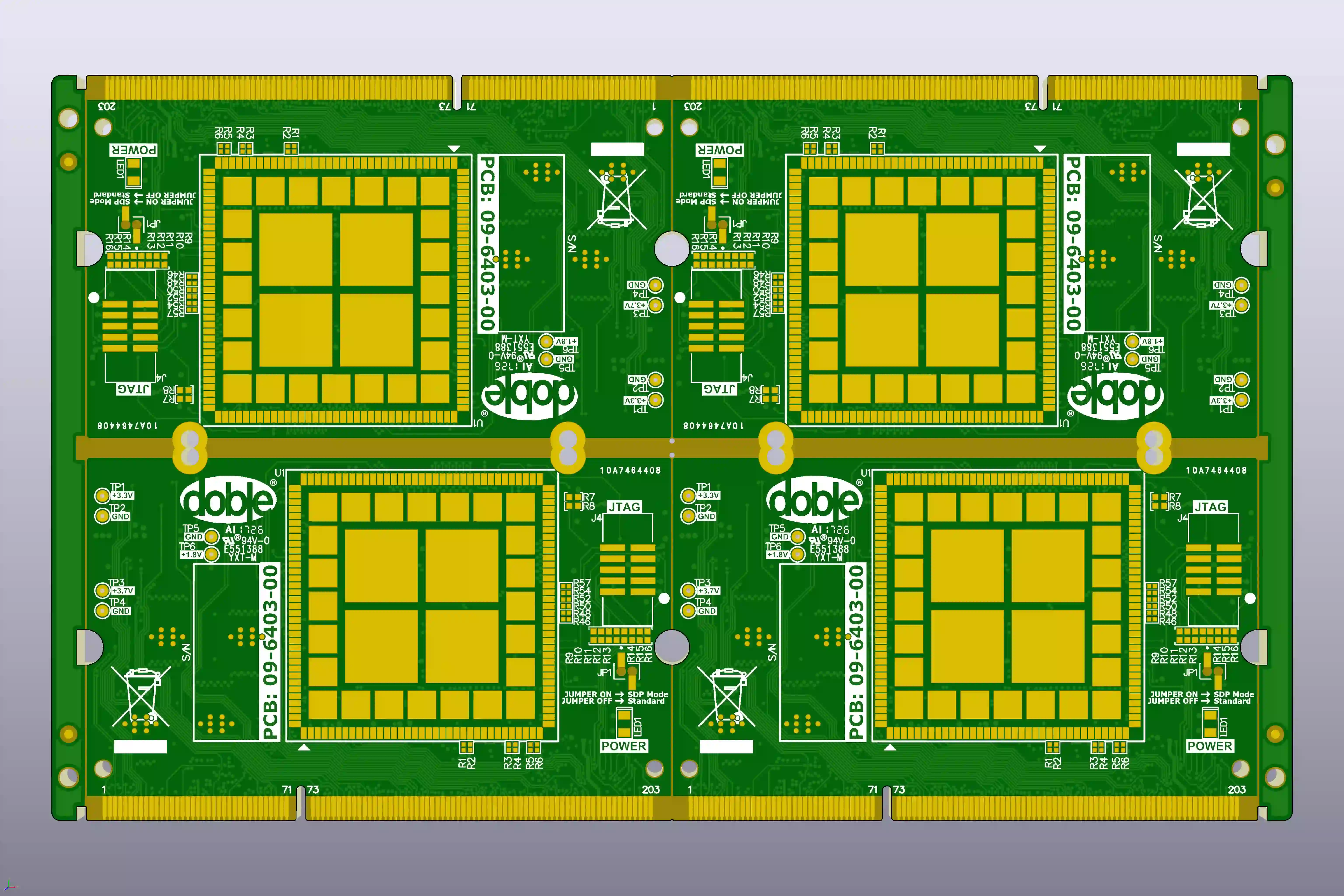
This 12-layer FR-4 PCB measured 235.13 × 259.7 mm with 2.0 mm thickness, TG170 material, and 1 oz copper on both sides. Produced as 10 single pieces, the order used ENIG surface finish (2 µin gold), red solder mask, and white silkscreen. The design included controlled impedance with a required report, resin-plugged vias, and 0.3 mm minimum holes at standard 6 mil line/space. Customer self-panel format and mechanical routing were specified, with a 19-day schedule that included 100% flying probe testing.
DFM review resolved several layer, material, and feature issues. One ART layer corresponding to an internal plane contained no data and required confirmation of intent. Back-drilling was noted to leave residual pits at the finished stage. Top-side vias carried full solder-mask openings rather than tenting. The specified M-890K and EM-89BK materials were unavailable and were replaced with equivalent Panasonic M6 while preserving performance targets. Certain holes appeared plated from the graphics yet were defined as NPTH, requiring attribute clarification. Batch and serial-number rules were incomplete, and some silkscreen characters were expected to be incomplete. Impedance control was limited to the traces that could be clearly identified in the data; unlocated impedance lines were excluded from compensation.
Confirmed material substitution, hole attributes, impedance scope, and marking decisions were implemented prior to production. The high-layer boards achieved consistent ENIG plating, reliable resin filling, and controlled impedance performance within the planned timeline. Full electrical test reports, impedance documentation, and quality certificates accompanied the shipment, confirming the panels met the specified mechanical and electrical requirements.
Explore More PCB Manufacturing Resources
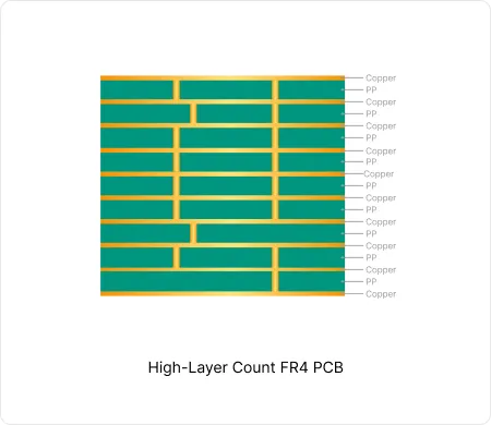
High-Layer Count FR4 PCB Manufacturing
These high-layer count FR4 PCB enable high-density interconnects while maintaining signal integrity and thermal reliability in computing and communication equipment.
How to Resolve Gold Finger Bevel and Impedance EQs in 10-Layer PCBs
Real 10-layer FR-4 case study: how CAM engineers resolved gold finger bevel clearance, impedance mismatch, tight via spacing and plugging risks to prevent scrap and signal integrity failures.
Real Production Records
| Order ID | PCB Type | Layers | Dimensions | Solder Mask | Surface Finish | Quantity | Action |
|---|---|---|---|---|---|---|---|
| FR4-20260919-046 | FR4 PCB | 2 | 76 x 374 | Matte Black | HASL Lead Free | 30 | View detail |
| FR4-20260918-033 | FR4 PCB | 6 | 55 x 41.7 | Green | ENIG (Immersion Gold) | 5 | View detail |
| FR4-20260912-059 | FR4 PCB | 2 | 275 x 193.7 | Green | ENIG (Immersion Gold) | 100 | View detail |


