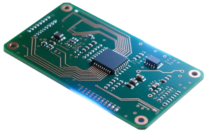
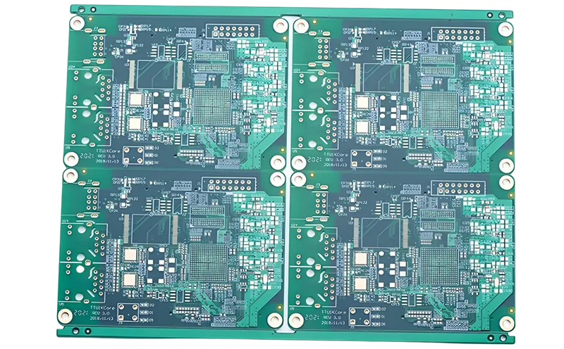
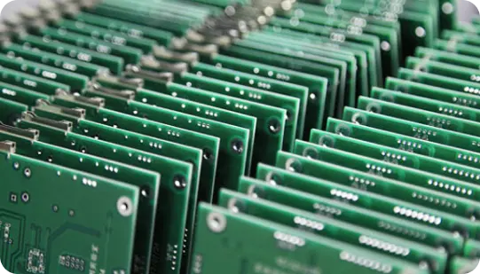
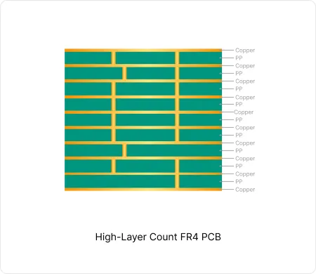
These high-layer count FR4 PCB enable high-density interconnects while maintaining signal integrity and thermal reliability in computing and communication equipment.
| Parameter | Typical Range |
|---|---|
| Layer count | 10 to 32 layers |
| Material type | High Tg FR4, mid Tg FR4 |
| Surface finish | ENIG, Immersion Silver, HASL |
| Thickness | 1.0-3.2 mm |
| Solder mask | Green, black, red, white, yellow, blue, purple, matte black, matte black |
| Copper thickness | 0.5 oz to 2 oz |
| Special features | Impedance control, backdrilling, blind and buried vias, sequential lamination |
Lamination: Sequential lamination builds thick panels. Precise temperature and pressure profiles minimize material movement and ensure registration.
Drilling and Plating: High aspect ratio holes require controlled parameters. Pulse plating achieves uniform copper thickness throughout barrel depth.
Surface Finish Logic: ENIG supports fine pitch assembly. Process controls prevent nickel corrosion and ensure solder joint reliability.
Risk Control: CTE mismatch management reduces delamination risk. First article cross-sections validate all critical parameters before volume runs.
| Order Quantity | Order Proportion | Estimated Price Level | Typical Lead Time |
|---|---|---|---|
| Prototype (<=30 pcs) | 67% | From $168 | From 6 days |
| Small volume (30-200 pcs) | 23% | From $209 | From 6 days |
| Mass production (>200 pcs) | 10% | From $347 | From 7 days |
| Order ID | PCB Type | Layers | Dimensions | Solder Mask | Surface Finish | Quantity | Action |
|---|---|---|---|---|---|---|---|
| Loading... | |||||||
AIVON medical device PCBs are high-reliability boards designed for healthcare applications. Built with strict quality control, biocompatible materials, and precise manufacturing, they ensure safety and accuracy. Suitable for diagnostic equipment, patient monitoring, and wearable medical devices, AIVON PCBs meet ISO and IPC medical standards.
AIVON provides high-reliability PCBs designed for civil aviation and aerospace applications, built to perform under extreme conditions such as vibration, temperature variation, and high-altitude environments. These PCBs are widely used in avionics systems, flight control modules, communication equipment, and satellite technologies. With advanced multilayer structures, heavy copper options, and high-temperature materials, our solutions are engineered to meet stringent reliability standards such as IPC-6012 Class 3.
AIVON telecommunication PCBs are high-performance boards designed for fast and stable signal transmission. Used in base stations, routers, satellite systems, and 5G infrastructure, they feature advanced materials and precision manufacturing to ensure low signal loss, accurate impedance control, and reliable high-frequency performance.
High-layer-count FR4 PCBs demand precise fabrication and tight process control. AIVON manages complex stackups with accurate layer registration, controlled impedance, and reliable interlayer connections. From intricate designs to volume production, our engineering expertise and quality control help deliver stable electrical performance and consistent board quality for demanding applications.
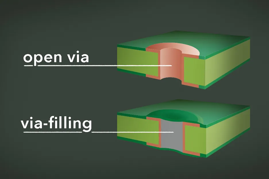
PCB filled vias deliver mechanical strength, thermal improvements, and reliability gains in high layer count PCBs. Details include via filling materials, reduced warpage effects, signal integrity benefits, fabrication practices, and standards for high reliability PCB designs used by electrical engineers.
Read More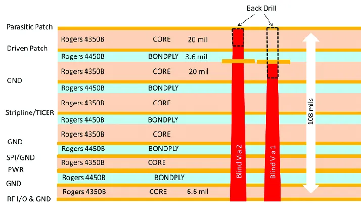
Cut PCB signal loss in high layer count RF PCB designs with proven stackup strategies and high frequency PCB materials. Covers dielectric losses, ground plane placement, symmetric layering, via optimization, and verification for reliable RF performance in dense boards.
Read More