










This was a 2-layer high-frequency board on Rogers RO4350B, 0.762 mm core, 51 mm by 165 mm, with 1 oz copper on both sides and immersion gold finish. Quantity was 50 pieces. The data package included stamp holes intended for breakaway tabs. During CAM review we found the hole-to-hole spacing measured only 0.267 mm. That number sits well below what our process can hold when the holes are plated through. The risk of board fracture during depanelization was real, so the spacing became the primary Engineering Question before any production could start.
Other items appeared as well—copper running closer than 0.2 mm to the outline, via-in-pad features, and a finished thickness target of 0.9 ± 0.1 mm—but the stamp-hole geometry was the one that could actually stop the board from surviving separation. We needed a clear capability decision: could the original spacing be kept, or did the design have to change to stay inside a stable manufacturing window?
Why 0.267 mm Stamp-Hole Spacing Failed on Rogers RO4350B PTH Boards
The order ( #ROG-20260331-007 ) original design showed stamp holes approximately 0.8 mm in diameter with center-to-center spacing of only 0.267 mm. The customer later confirmed the holes should be plated through. On a Rogers RO4350B laminate the combination is problematic. Plated holes add copper and therefore some strength, yet the remaining laminate bridge between holes becomes extremely narrow. Under the mechanical stress of routing or manual breakaway, that thin web is the first place to crack.
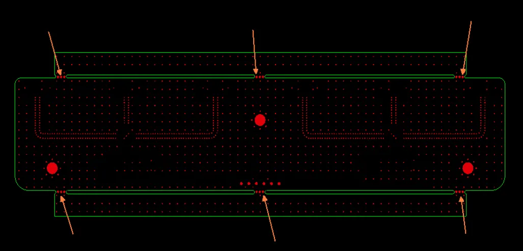
Figure 1: the stamp holes indicated by the arrows
We measured the gerber data and confirmed the 0.267 mm gap. Typical process capability for PTH stamp holes on high-frequency material requires a minimum web of about 0.4 mm after plating to keep fracture risk low. At 0.267 mm the residual material is simply too thin. Board breakage during depanelization is a realistic outcome, not a theoretical one. That is why the spacing triggered a formal EQ.
After internal review we proposed reducing the mouse-bites diameter from 0.8 mm to 0.5 mm and increasing the hole-to-hole spacing to 0.4 mm. The smaller holes still provide the breakaway function while restoring enough laminate between them to survive separation. We asked the customer to confirm the change before tooling.
| Parameter | Original Design | Proposed Change | Capability Assessment |
|---|---|---|---|
| Stamp hole diameter | 0.8 mm | 0.5 mm | Still functional for breakaway |
| Hole-to-hole spacing | 0.267 mm | 0.4 mm | Minimum reliable web for PTH on RO4350B |
| Plating type | PTH (customer confirmed) | PTH | Acceptable once spacing is corrected |
Why Rogers RO4350B Makes the Spacing More Critical
Rogers RO4350B is a ceramic-filled hydrocarbon laminate. It machines cleanly but has lower fracture toughness than standard FR-4 in thin sections. When the remaining web between plated holes drops below roughly 0.35–0.4 mm, the risk of micro-cracks during routing or snap separation rises sharply. On FR-4 the same geometry might survive; on RO4350B it often does not.
We also had to consider the finished board thickness. The core is supplied at 0.762 mm. With 1 oz finished copper the total thickness was to be controlled at 0.9 ± 0.1 mm. That call-out is achievable, but it means the plated copper itself becomes part of the mechanical structure around the stamp holes. If the laminate web is already marginal, the added copper stiffness can actually concentrate stress rather than relieve it. Keeping the spacing at 0.4 mm restores a safer process window.
IPC-6012 and common high-frequency fabrication practice both emphasize adequate material between breakaway features. The original 0.267 mm spacing fell outside those practical limits, which is why we could not release the design as drawn.
Copper-to-Outline Clearance Below 0.2 mm
A second issue appeared along the board edge. In several locations copper ran closer than 0.2 mm to the final outline. After mechanical routing the remaining copper can be left exposed or partially peeled. On immersion-gold boards this often shows as edge copper or "rolled copper" defects. We flagged the clearance and asked for confirmation that the design intent accepted the risk, or that the copper should be pulled back.
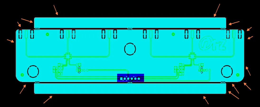
Figure 2: the copper clearance from the board outline is less than 0.2mm per side
For high-frequency circuits even a small edge anomaly can affect RF performance if it sits near a critical trace. The safer manufacturing choice is to maintain at least 0.25–0.3 mm copper-to-outline clearance so the router leaves a clean, fully covered edge. The customer needed to decide whether to accept the original geometry or adjust it.
Via-in-Pad Features and Solder-Mask Openings
Multiple vias were placed inside pads. On a 2-layer Rogers board this is manufacturable provided the via diameter and pad size allow reliable plating and the subsequent solder-mask or surface-finish process can close or protect the via as intended. We asked for confirmation that the via-in-pad design was deliberate. No special process such as via filling was specified, so standard plated vias with tenting or open mask were assumed.
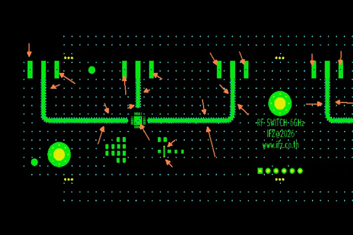
Figure 3: multiple locations have via-in-pad design
A few silkscreen symbols also sat over solder-mask openings. The characters would be printed into the open area. We noted the condition so the customer could verify the marking would still be legible after gold plating and final finish.
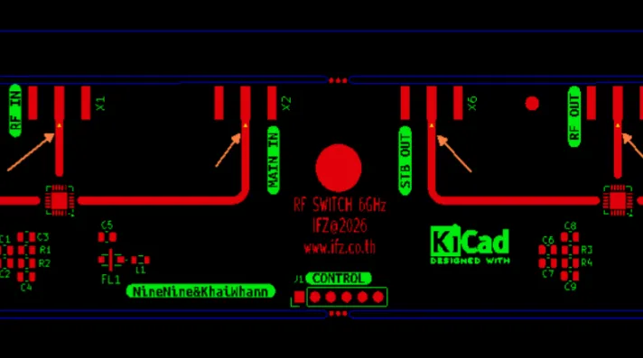
Figure 4: the symbol at the location indicated by the arrow is designed on top of the opening
These items were secondary. They did not threaten board integrity the way the stamp-hole spacing did, so they required only confirmation rather than a redesign proposal.
| Issue | Observed Condition | Process Risk | Action Taken |
|---|---|---|---|
| Stamp hole spacing | 0.267 mm web | High fracture risk on RO4350B | Propose 0.5 mm hole / 0.4 mm spacing |
| Copper-to-outline | < 0.2 mm | Exposed or rolled copper after routing | Request confirmation or pull-back |
| Via-in-pad | Multiple locations | Standard if plating is reliable | Confirm design intent |
| Finished thickness | 0.9 ± 0.1 mm target | Achievable with 0.762 mm core + 1 oz Cu | Control plan locked |
Verifying 0.5 mm Holes at 0.4 mm Spacing Inside the RO4350B Process Window
Before sending the revised stamp-hole proposal we verified that 0.5 mm holes at 0.4 mm spacing sit inside our normal process window for Rogers RO4350B. Drill capability for 0.5 mm holes on 0.762 mm material is routine. After plating the remaining web is approximately 0.4 mm, which has proven stable in previous high-frequency depanelization runs. Mechanical routing of the outline with no process edge (0 mm) is also standard once copper clearance is acceptable.
We also confirmed the thickness control plan. Starting from a 0.762 mm core and building to 1 oz finished copper produces a nominal thickness near 0.9 mm. Holding ±0.1 mm is within normal lamination and plating variation for this material. No special process steps were required beyond the usual thickness mapping on first articles.
The combination of corrected stamp-hole geometry, verified thickness window, and confirmed copper-edge treatment brought every critical parameter back inside a repeatable capability range.
First-Article Validation Approach
Once the customer approved the reduced stamp-hole diameter and 0.4 mm spacing, first-article panels were built. We measured the actual hole-to-hole web after plating and confirmed it met the 0.4 mm target. Depanelization trials on sample pieces showed clean breaks with no cracks propagating into the circuit area.
Thickness was checked at multiple points across the panel; all readings fell inside 0.9 ± 0.1 mm. Edge inspection after routing verified that any locations still carrying copper closer than 0.2 mm were noted, but no peeling or exposure occurred beyond the accepted risk level. Via-in-pad plating was cross-sectioned and found continuous. The process window held.
| Validation Item | Method | Result |
|---|---|---|
| Stamp-hole web after plating | Optical measurement | ≥ 0.4 mm, no fracture in depanel trials |
| Finished thickness | Micrometer + laser gauge | Inside 0.9 ± 0.1 mm |
| Copper edge after routing | Visual + magnification | No uncontrolled peeling |
| Via-in-pad plating | Cross-section | Continuous copper |
Final Capability Decision
The original 0.267 mm stamp-hole spacing on plated holes exceeded the process capability of Rogers RO4350B for reliable depanelization. Reducing the hole diameter to 0.5 mm and setting the spacing to 0.4 mm restored a stable manufacturing window. The finished thickness target of 0.9 ± 0.1 mm was confirmed achievable from the 0.762 mm core with 1 oz copper. Copper-to-outline clearances below 0.2 mm were left for customer acceptance or minor adjustment, and via-in-pad features were verified as standard.
With these clarifications locked, the board moved into production under normal process controls. The case shows why stamp-hole geometry must be checked against the actual laminate and plating stack before release: a spacing that looks acceptable on screen can still sit outside the physical limits of the material once the holes are plated and the panel is routed.
FAQ
Q1: Why is 0.267 mm stamp-hole spacing a problem on Rogers RO4350B?
After plating, the remaining laminate web becomes extremely thin. Rogers RO4350B has lower fracture toughness than FR-4 in narrow sections. Under routing or breakaway stress the thin web can crack and the crack can run into the circuit. A minimum 0.4 mm web after plating is the practical lower limit for reliable separation on this material.
Q2: Why reduce the stamp-hole diameter from 0.8 mm to 0.5 mm?
Smaller holes leave more laminate between them when the center-to-center distance is increased to 0.4 mm. The 0.5 mm diameter still functions as a breakaway feature while restoring enough material strength to prevent fracture during depanelization.
Q3: Can copper running closer than 0.2 mm to the outline be accepted?
It can be accepted if the customer understands the risk of exposed or rolled copper after mechanical routing. For high-frequency boards the safer practice is to maintain at least 0.25–0.3 mm clearance so the finished edge remains fully covered by solder mask or gold. The decision belongs to the designer once the manufacturing risk is clear.
Q4: Is a finished thickness of 0.9 ± 0.1 mm realistic on 0.762 mm Rogers RO4350B?
Yes. Starting from the 0.762 mm core and building 1 oz finished copper on both sides produces a nominal thickness near 0.9 mm. Normal process variation stays inside ±0.1 mm when lamination and plating are controlled. Thickness mapping on first articles confirms the window.
Q5: Do via-in-pad features require special processing on this 2-layer board?
Not necessarily. Standard plated vias are acceptable if the via diameter and pad size allow reliable copper coverage. No via-fill or special plugging was specified, so the process stays within normal capability once plating quality is verified by cross-section.
Q6: Why treat PTH stamp holes more carefully than NPTH stamp holes?
Plated holes add copper stiffness. When the remaining laminate web is already narrow, the plated copper can concentrate stress instead of reinforcing the joint. NPTH holes leave only the laminate, which can sometimes tolerate slightly tighter spacing, but once the customer specifies PTH the spacing must be opened to keep the web strong enough for clean separation.






