










A 6-layer FR-4 board measuring 142.4 mm × 219.6 mm came in for CAM review. The order specified 1.6 mm finished thickness, TG170 material, 3 oz copper on every layer, green solder mask on both sides,no silkscreen, immersion gold, resin-plugged vias, and a customer-supplied 1 × 4 panel. Quantity was 300 pieces across 75 sets. The customer note stated that milling should follow MILLING.gbr and that both the stackup and the final thickness should follow STACKUP.png. When we calculated the stack from the supplied drawing, the finished thickness came out to 1.5 mm. At the same time we had no Shengyi TG170 core in stock and needed to substitute NP-175FTL. These two facts created a direct conflict between the ordered thickness, the customer's own stackup file, and the material we could actually use. We could not release the job until the final stackup and thickness were confirmed.
Why High-Copper 6-Layer Designs Demand Exact Thickness Control
The board ( #FR4-20260407-027 ) was a high-copper, high-density 6-layer design. Three-ounce copper on all layers is uncommon and usually chosen for current-carrying capacity or thermal performance. Resin-plugged vias were specified, which is typical when the surface needs to stay flat for fine-pitch components or for reliable immersion-gold plating. The panel was customer-defined in a 1 × 4 array with routing slots and zero process edge. The designer clearly expected the finished board to measure 1.6 mm after pressing and plating. The STACKUP.png file was supplied as the controlling document for how that thickness should be built. In normal practice the stackup drawing and the ordered thickness should agree. In this case they did not.
Thickness Calculation and Material Shortage
We reconstructed the press structure exactly as shown in STACKUP.png. Core thicknesses, prepreg counts, and copper weights were entered into the calculation. The result was a nominal finished PCB thickness of 1.5 mm after accounting for copper plating and solder-mask thickness. That is 0.1 mm below the 1.6 mm stated in the order. On a board with 3 oz copper the difference is not trivial. The heavier copper already reduces the dielectric thickness available between layers. A further 0.1 mm reduction changes the overall board height and can affect connector engagement, mechanical fit in the enclosure, and even the residual dielectric thickness that remains after plating.
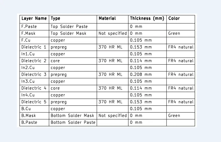
Figure 1: laminated structure provided by customer
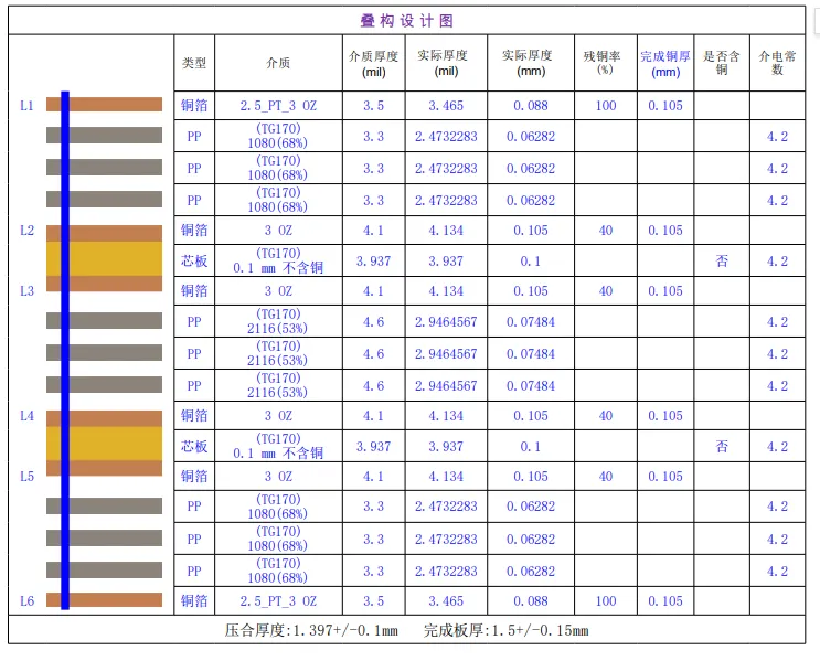 Figure 2: our laminated structure
At the same time our inventory check showed no Shengyi TG170 core. The only available high-Tg alternative that could meet the thermal and electrical requirements was NP-175FTL. This material has a different resin system and a slightly different pressed thickness for the same core construction. Using it forced us to redraw the entire press structure. The new stack still aimed for 1.6 mm, but the dielectric distribution and the final tolerance window changed. We could not assume the customer would accept either the 1.5 mm result from the original drawing or the new material without explicit confirmation.
If we had shipped boards at 1.5 mm, they would have been out of the ordered thickness. If we had waited for Shengyi TG170 core, the 13-day lead time would have been missed. Both options created real risk for a 300-piece order.
| Source | Thickness | Material | Issue |
|---|---|---|---|
| Order parameters | 1.6 mm | Shengyi TG170 | Stated target |
| STACKUP.png calculation | 1.5 mm | As drawn | 0.1 mm short of order |
| Factory stock | — | NP-175FTL only | Forced material change |
Why the Stackup Conflict Blocked Production
The conflict sat at the intersection of three documents. The order said 1.6 mm. The STACKUP.png file produced 1.5 mm when calculated correctly. The material we could buy forced a third construction. In CAM practice the stackup drawing is normally the controlling document for dielectric build. When that drawing does not deliver the thickness written in the order, the factory cannot decide which number to target. Changing the core material adds another variable because different resins press to slightly different final thicknesses even when the nominal core construction looks the same.
On a 6-layer board with 3 oz copper the dielectric layers are already thin. A 0.1 mm overall error can reduce the distance between internal planes enough to affect voltage withstand or to change the mechanical stiffness of the board. It can also push the finished height outside the tolerance of a card-edge connector or a press-fit housing. Because the customer had supplied the stackup drawing as the reference, we could not simply ignore it and force 1.6 mm with the original material. We also could not ship 1.5 mm boards without approval. The only safe path was to present both the calculated result and the revised NP-175FTL stack and let the customer choose.
Further review showed that the original STACKUP.png did not include a clear tolerance. Without a tolerance band we had no way to know whether 1.5 mm was already inside the customer's acceptable window or whether 1.6 mm was a hard minimum. That ambiguity alone was enough to stop the job.
Production Number Placement, 0.8 mm Panel Tabs, and Missing Paste Layer Risks
While the stackup was the main blocker, three other points appeared in the same review. The production notes asked for a production number on every board, yet the Gerber set contained no silkscreen or text layer. The only remaining surface that could carry permanent marking was the solder mask. We needed permission to place the number there without reducing clearance or overlapping copper.
The panel used routing slots and zero process edge. The connection tabs between boards measured only 0.8 mm. That width is workable, but it leaves little margin during depaneling. A routing bit that wanders even slightly can break into the functional board area. We asked the customer to confirm that the 0.8 mm spacing was intentional and that they accepted the higher risk of edge damage.
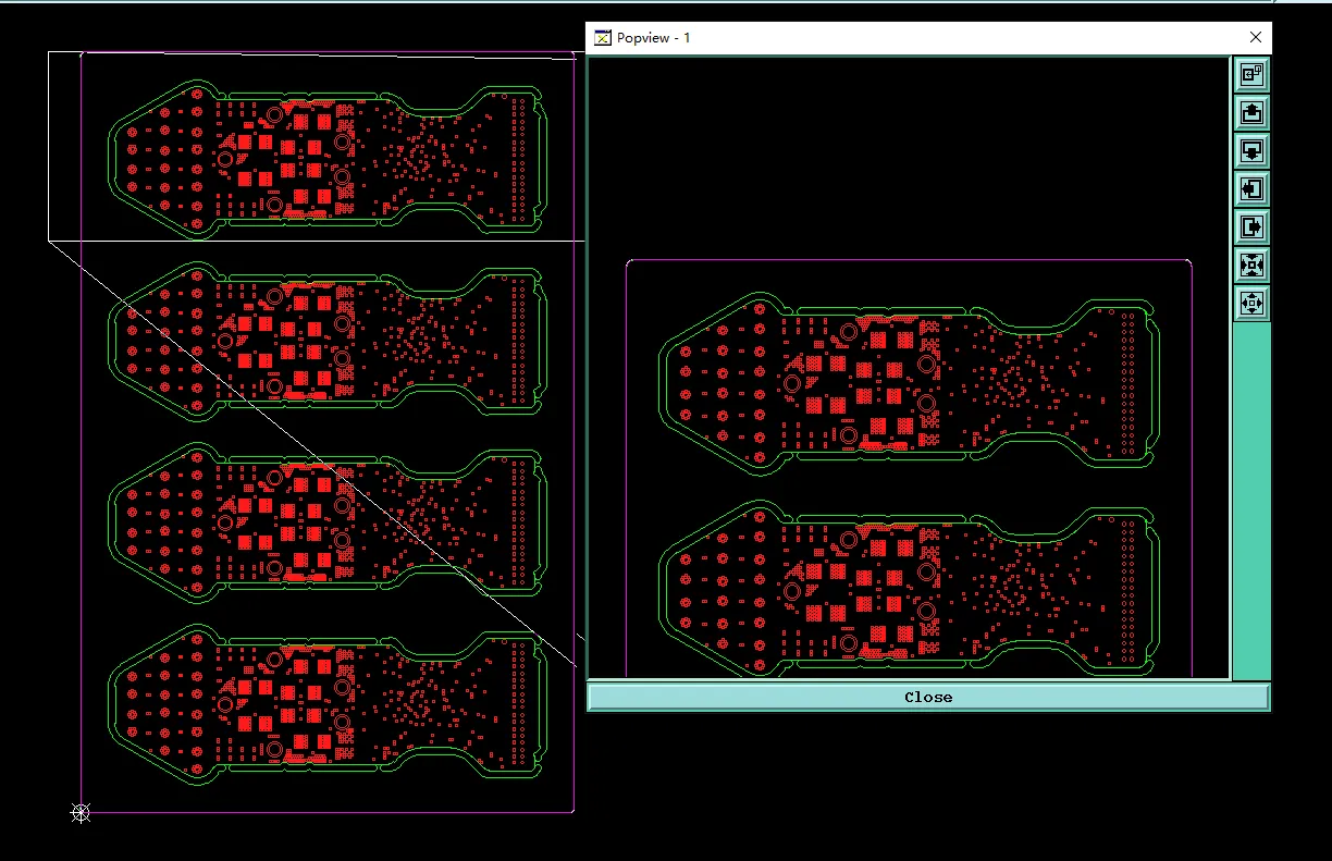
Figure 3: The connection tabs between boards measured only 0.8 mm
Finally, the notes mentioned a solder-paste layer and the need to return a stencil file with the production data. No paste layer existed in the Gerber package. Without the layer we could not generate a stencil file. These three items were secondary, but each of them required a clear answer before the job could be considered fully released.
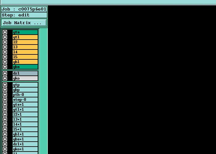
Figure 4: No paste layer existed in the Gerber package
Customer-Approved NP-175FTL Stack and Solder-Mask Marking Solution
We prepared a short engineering reply that contained three concrete proposals. First, we showed the 1.5 mm thickness that resulted from the original STACKUP.png and asked whether that value was acceptable. Second, we supplied a complete revised press structure that used NP-175FTL and adjusted core and prepreg thicknesses to come as close as possible to 1.6 mm. The new stack included the expected pressed tolerance so the customer could see the realistic finished range. Third, we asked for permission to place the production number on the solder-mask layer in a location that preserved clearance.
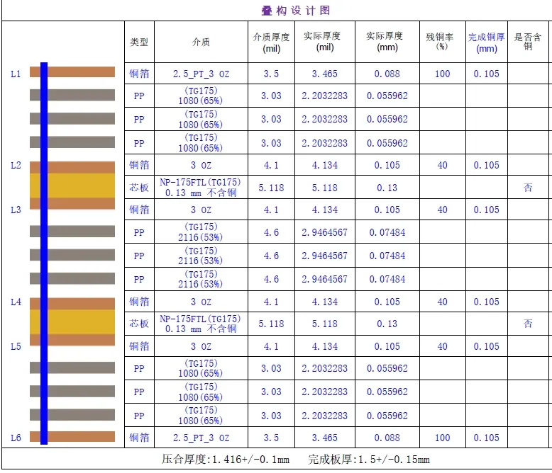
Figure 5: final lamination structure
We also confirmed that the 0.8 mm panel tabs would be processed exactly as drawn and that no stencil file could be generated because no paste layer was present. The reply was written so the customer could approve or reject each point independently.
The customer accepted the NP-175FTL substitution and the revised press structure. The production number was allowed on the solder mask. The panel tabs and the missing paste layer were accepted without change. Once those answers were in hand, the CAM data were updated, the press program was locked, and the 75-panel order was released to production.
| Observation | Conflict | Proposal | Final Decision |
|---|---|---|---|
| STACKUP.png calculates to 1.5 mm | Order requires 1.6 mm | Offer revised NP-175FTL stack aimed at 1.6 mm | Approved |
| No Shengyi TG170 core available | Material change required | Substitute NP-175FTL and redraw press | Confirmed |
| No text layer for production number | Marking location undefined | Place number on solder mask | Accepted |
| 0.8 mm panel tabs with zero edge | Tight for routing depanel | Process exactly as drawn | Accepted |
Design Checks That Prevent Thickness and Material Confirmation Delays
- When you supply a STACKUP.png, run the thickness calculation yourself before release. Make sure the result matches the thickness written in the order.
- If the material you specify might be out of stock at the fabricator, list one or two acceptable alternates in the fabrication notes. That single line can save days of back-and-forth.
- On thick-copper 6-layer boards a 0.1 mm thickness error is large enough to affect mechanical fit. Treat the thickness as a hard requirement and give a tolerance.
- If a production number is required and no silkscreen layer exists, state clearly that the number may be placed on the solder mask and indicate an acceptable location.
- Panel tabs of 0.8 mm with zero process edge are possible, but they raise the risk of breakout during routing. Confirm that the customer accepts that risk.
- Notes that refer to a solder-paste layer should be accompanied by an actual paste layer in the Gerber data. Without the layer the factory cannot generate a stencil file.
- Always include a thickness tolerance when the nominal value is critical. A bare "1.6 mm" leaves the factory without a decision window.
- High copper weights reduce the dielectric thickness available between layers. Small overall thickness errors therefore have a larger relative effect on internal spacing.
FAQ
Q1: Why does a 0.1 mm difference between ordered thickness and calculated stackup matter on a 6-layer board?
A1: With 3 oz copper the dielectric layers are already thin. An extra 0.1 mm reduction changes overall board height, can affect connector engagement, and reduces the residual dielectric between internal planes. It is large enough to require customer approval.
Q2: What happens when the specified core material is out of stock?
A2: The factory must propose a substitute material and a new press structure. Production stops until the customer confirms both the material change and the revised stackup. Listing acceptable alternates in the original notes avoids this delay.
Q3: Can a production number be placed on the solder mask when no silkscreen layer exists?
A3: Yes, provided the customer agrees and the chosen location does not reduce electrical clearance or overlap critical copper features. The factory will not place the mark without that permission.
Q4: Is 0.8 mm tab spacing safe for a routing-slot panel with zero process edge?
A4: It is tight. The routing bit has little room for wander. The risk of breakout into the functional board is higher than with wider tabs. The customer must explicitly accept that risk if the design stays unchanged.
Q5: Why can't the factory generate a stencil file when the notes mention a solder-paste layer?
A5: No paste layer exists in the Gerber data. Without the layer there is nothing to convert into a stencil file. The note cannot be fulfilled as written.
Q6: How can designers avoid stackup confirmation delays on thick-copper boards?
A6: Calculate the finished thickness from the stackup drawing before release and make sure it matches the order. List acceptable alternate materials. Include a thickness tolerance. These three steps eliminate most of the back-and-forth that appeared in this case.






