










When a rigid-flex PCB combines thin polyimide flexible cores with FR-4 rigid sections, the CAM review stage becomes the primary filter that protects both yield and long-term reliability. In this order the customer specified a 7-layer construction (approximately five flexible layers plus two outer rigid layers), black coverlay on the flex region, black solder mask with white legend on the rigid region, ENIG surface finish, and IPC Class 3 acceptance. The design also carried strict outgassing limits on the solder mask (ASTM E595) and requested PI stiffeners without clear location data. Our engineering team opened the files and immediately encountered a series of inconsistencies between the fabrication notes, the Gerber layers and the material call-outs. The following case study records the actual EQ process, the manufacturing risks that would have remained if clarification had been skipped, and the final agreements that allowed the job to be released.
7-Layer Rigid-Flex Order Specs and Class 3 Process Limits
The board ( #RFP-20260707-040 ) measures 256.23 mm × 67.05 mm and was ordered as 10 pieces. Overall rigid thickness was specified as 1.6 mm; the flexible section total thickness after lamination was targeted at approximately 0.5 mm. Copper weight on the outer layers was 1 oz while the inner flexible copper was 0.5 oz. Surface finish was ENIG with 1.0 µin gold over 120–200 µin nickel. Vias were required to be tented with solder mask. Delivery was single-piece (no panelization), flying-probe full electrical test, and a full set of IPC Class 3 reports including microsection analysis and thermal-stress evaluation. The customer explicitly referenced Shengyi SF202 (or equivalent Pyralux AP) for the flexible core and requested PI stiffeners. Lead time was quoted at 27 calendar days with an internal target of 17–18 working days. The order also carried an SMT request for two connectors, J1 and J2, although only J2 material was supplied.
From a process viewpoint the construction is a classic rigid-flex hybrid: laser-routed outline, no V-score, positive etch, and no impedance control. The combination of thin polyimide, mixed copper weights, and Class 3 cleanliness requirements already places the design near several manufacturing limits. That is why the CAM review generated more than a dozen engineering questions before any panel could be released.
Critical CAM Conflicts That Blocked Release of the Rigid-Flex Panel
Why Mixed Copper Weights and Unclear Adhesives Forced a Full Stackup Rebuild
The original fabrication notes mixed 0.5 oz and 1 oz copper call-outs and listed both Pyralux AP and generic FR-4 materials. Our CAM engineer rebuilt the stackup using the physical layer count visible in the Gerber files and adjusted the rigid section to 1.6 ± 0.16 mm and the flexible section (after coverlay) to 0.5 ± 0.05 mm. Inner copper was standardized at 0.5 oz and outer copper at 1 oz. Flexible material was changed to Shengyi SF202 (an accepted equivalent to Pyralux AP under IPC-4103 guidelines) and the rigid cores were switched to S1000-2. Coverlay was also specified as Shengyi product.
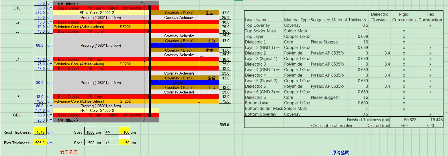
Figure 1: confirming stack-up and materials
We asked the customer to confirm the revised stackup and material list. If production had continued with the original mixed copper weights, the etch factor on the thin flexible copper would have been inconsistent with the heavier outer copper, producing undercut or over-etch on the fine traces and risking open circuits or reduced current-carrying capacity. In a Class 3 rigid-flex PCB design that kind of thickness variation can also create residual stress that later appears as delamination after thermal cycling.
After reviewing the stackup, we found that the customer's original notes did not clearly define the adhesive systems between the flexible and rigid sections. We therefore locked the materials to the Shengyi family so that the glass-transition and expansion coefficients remained matched, reducing the risk of warpage that is common when dissimilar polyimide and FR-4 systems are laminated together.
Why Undefined 0.2 mm PI Stiffeners Were Recommended for Deletion
The fabrication drawing called for PI stiffeners of 0.2 mm thickness, yet neither the Gerber data nor the mechanical drawing contained coordinates or outline dimensions for those stiffeners. Our engineer suggested that the stiffener requirement be ignored for this particular design. In our experience a PI stiffener is normally placed on the reverse side of an area that carries component pads or connectors so that the flex region remains flat during assembly. On this board the flexible zone contained only mesh copper and routing traces; no component openings existed in the soft region. Adding an undefined stiffener would have required guessing the location, risking either insufficient support or interference with the final outline.
If the stiffener had been fabricated in an arbitrary position, the additional local thickness could have caused the laser-routed outline to drift or created an uneven pressure distribution during coverlay lamination, leading to resin voids or incomplete adhesion. We therefore recommended omitting the stiffener entirely and asked for explicit customer confirmation.
Via Tenting Conflict: Open Windows vs. Full Cover and 0.2 mm Hole Risks
The order notes clearly required vias to be tented with solder mask. The Gerber solder-mask layers, however, showed double-sided openings over the majority of the vias. Our CAM team identified the conflict and proposed to delete the via openings and process the board as fully tented. In addition, three 0.6 mm vias were highlighted; these holes would inevitably show a slight red ring at the copper-solder-mask interface and a small amount of ink accumulation inside the barrel after tenting. We asked the customer to accept that cosmetic condition.
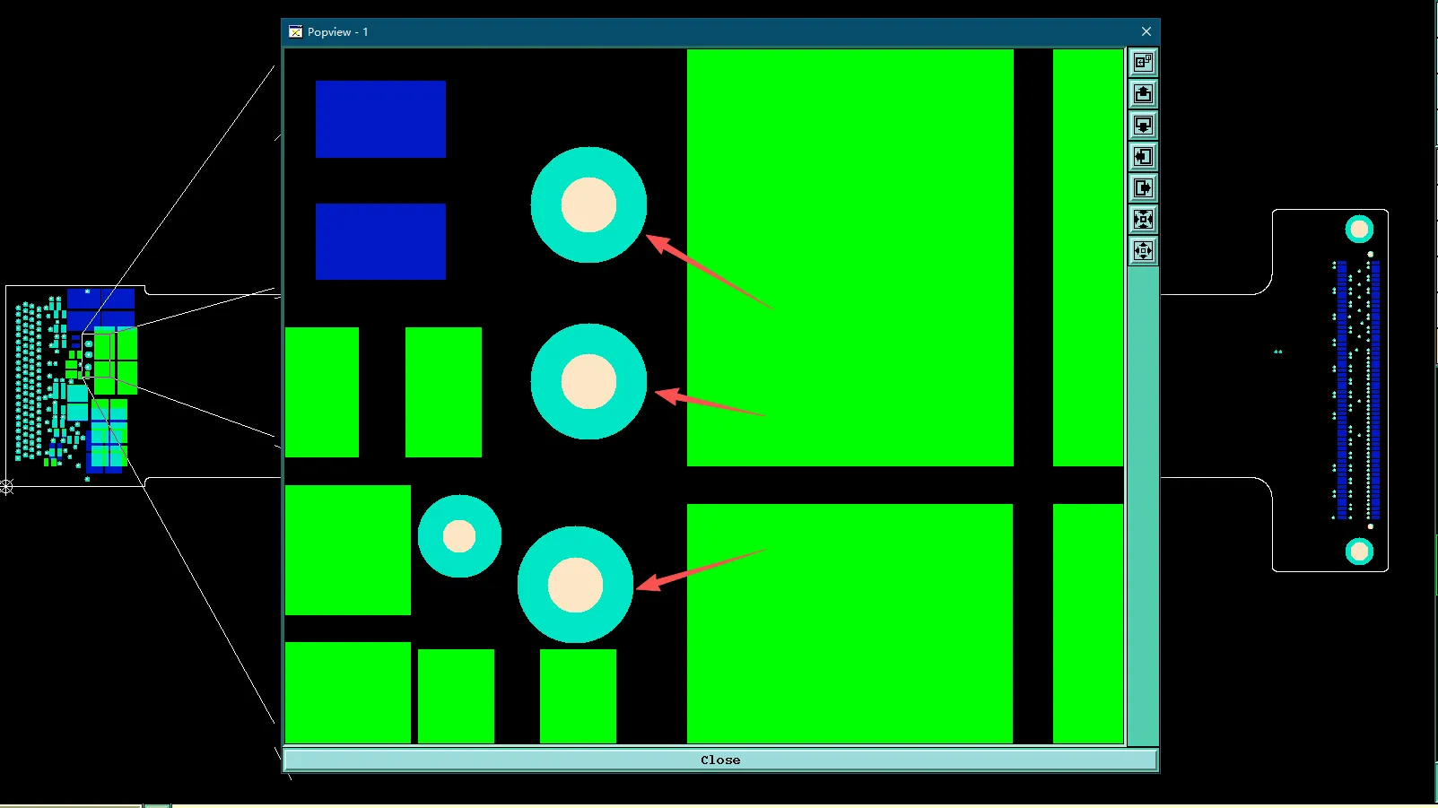
Figure 2: the original design shows double-sided via openings
A second via-related risk appeared on the 0.2 mm holes. Even if the customer insisted on open windows, the small diameter makes complete development of the solder-mask resist unreliable. Residual ink can remain inside the hole, creating a plugged via that later fails electrical continuity or traps flux during assembly. Our engineer therefore requested written acceptance of possible incomplete development on those small vias.
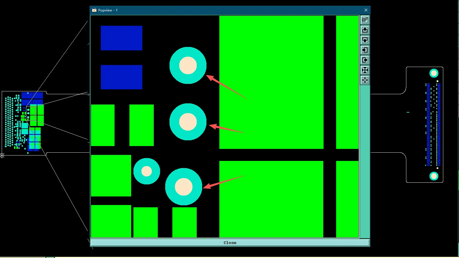
Figure 3: some vias (0.2 mm) may experience incomplete development during solder mask application due to their small diameter
If the tenting-versus-open conflict had been ignored, the finished boards could have left the factory with exposed copper around the via mouths. During subsequent handling or conformal-coating processes that copper is easily contaminated, raising the probability of dendritic growth or intermittent shorts under humidity. For the 0.2 mm holes the risk of permanent plug-up would have translated directly into open-circuit rejects at flying-probe test, lowering overall yield.
Why Black Solder Mask Failed ASTM E595 and Forced a Green Conversion
The customer's member notes required the solder mask to meet ASTM E595 limits (TML ≤ 1.0 % and CVCM ≤ 0.1 %). Our available black solder mask (PSR-2000 series) could not be certified to those outgassing values. The only system that met both the color preference and the ASTM numbers was the green PSR-4000 GEC50A / CA-40 G50 combination. We therefore recommended converting the rigid-section solder mask from black to green while keeping the flexible coverlay black as originally requested.
We noticed that the original black-ink call-out conflicted with the outgassing clause in the same document set. If production had continued with non-compliant black ink, the finished boards would have failed any subsequent vacuum or thermal-vacuum bake-out test, rendering the entire lot unusable for the intended high-reliability application. Changing to the green system eliminated that risk while still providing the required IPC Class 3 solder-mask adhesion and coverage.
Failure Modes That Would Have Appeared if EQ Clarification Had Been Skipped
Comparison of the GBP and GBS layers revealed three additional pads present only on GBP. We asked whether those pads should be fabricated. In parallel, the customer requested date code, factory code and serial number to be added at "specified positions," yet no coordinates or text content were supplied. Our engineer suggested omitting the variable marking to avoid incorrect placement.
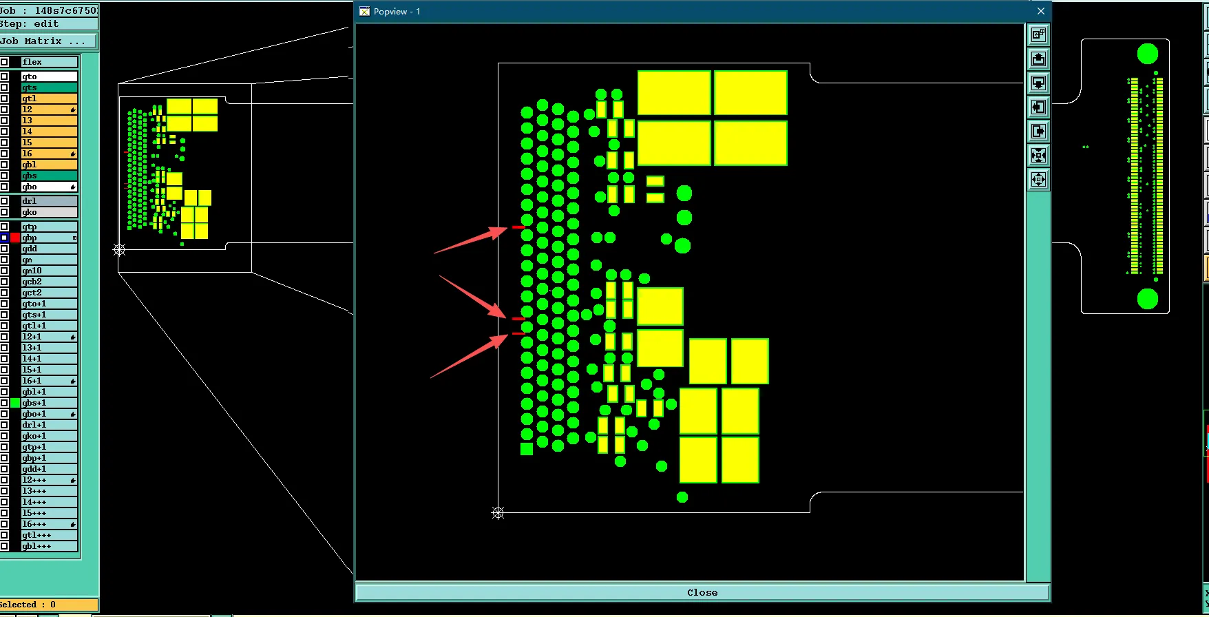
Figure 4: the GBP layer has three additional pads (indicated by the red arrow) compared to the GBS layer
To improve coverlay-to-copper adhesion on the flexible inner layers we proposed adding a small number of independent copper pads (shown in green on the review plot). These floating pads increase the local bond area without affecting electrical function. The customer was asked to confirm acceptance of the added pads.
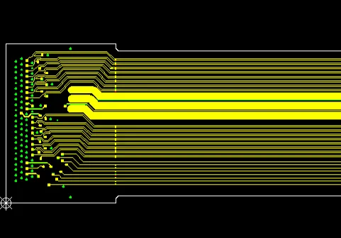
Figure 5: isolated pads (green pads) are added on the inner layers
Finally, the SMT request listed both J1 and J2. Only J2 material arrived; J1 was missing. We confirmed that J1 would not be placed and that no solder would be applied to its pads, while J2 had already been mounted. Written acceptance of the incomplete assembly was requested before final packaging.
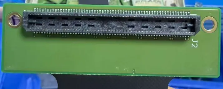
Figure 6: a model for J2 (BTE-060-01-F-D-A)
Manufacturing Risks and DFM Insights
This case illustrates several recurring rigid-flex pitfalls. First, mixed copper weights without a clear layer-by-layer table force the CAM engineer to choose a single etch recipe; the wrong choice produces either undercut fine lines or residual copper that later causes shorts. Second, undefined stiffener geometry is almost always resolved by omission, yet the customer may later discover that the flex region needs local rigidity for connector insertion. Third, solder-mask openings over small vias create a classic process conflict: the same feature cannot be both tented for cleanliness and open for probe access. Fourth, specifying an ink color that cannot meet the outgassing standard written in the same document set is a documentation inconsistency that only becomes visible during material verification.
If any of these items had been left unresolved, the most probable outcomes would have been:
- Delamination at the rigid-flex interface after thermal stress testing because of mismatched material systems.
- Via barrel cracking or incomplete plating on the 0.2 mm holes caused by residual solder-mask ink.
- Exposed copper at via mouths leading to edge shorting or contamination during assembly.
- Complete lot rejection after ASTM E595 outgassing measurement.
- Yield loss at flying-probe test from plugged micro-vias.
- Cosmetic and functional rejects from incorrectly placed stiffeners or missing serial marking.
Each of these failure modes is expensive because the boards are already at final thickness and surface finish when the defect is discovered. Early EQ resolution is therefore the only practical way to protect both schedule and cost.
How the Engineering Team Resolved the Issues
Our engineering team prepared a consolidated EQ package that grouped the questions by process impact. The revised stackup drawing was issued first so that material procurement could begin while the remaining items were still under discussion. For the stiffener we supplied a short technical note explaining why the mesh-copper region did not require local reinforcement and recommended deletion. On the via question we generated a color-coded plot showing the three 0.6 mm holes that would exhibit red-ring and ink accumulation, together with a process capability statement for the 0.2 mm holes. The solder-mask color change was supported by the actual ASTM E595 certificates of the green system. The three extra pads on GBP were flagged for customer decision, and the independent adhesion pads were shown as optional DFM improvements. Finally, the SMT status of J1/J2 was documented with photographs of the partially assembled panel.
All answers were received within the same working day. The customer accepted the SF202 / S1000-2 stackup, agreed to omit the PI stiffener, approved full tenting of vias (including the cosmetic conditions on the 0.6 mm holes), accepted the risk statement for the 0.2 mm holes, approved the change to green solder mask on the rigid sections, confirmed the three extra pads should be fabricated, accepted the added adhesion pads, waived the variable marking, and agreed that J1 would remain unpopulated. With every critical parameter locked, the CAM data were updated, the panelization program was finalized, and the job was released to the production floor.
After the EQ cycle the board entered fabrication with a fully consistent data package. Rigid thickness, flexible thickness, copper weights, materials, via treatment, solder-mask system and assembly status were all documented and customer-approved. No further engineering holds occurred. The panels completed lamination, laser outline, ENIG plating and flying-probe test without the yield losses that the original data conflicts would have produced. Microsection reports confirmed the agreed layer thicknesses and via structures, and the boards were shipped as single pieces with the required IPC Class 3 documentation.
Design Rules That Prevent Rigid-Flex CAM Holds and Yield Loss
- Provide a complete layer-by-layer stackup table that lists copper weight, dielectric type and thickness for every layer; mixed call-outs force the factory to make assumptions that may not match design intent.
- If PI stiffeners are required, include both the outline and the exact coordinates in the mechanical drawing or a separate stiffener Gerber; otherwise the feature will be omitted.
- Decide early whether vias are to be tented or open and make the solder-mask layers match the fabrication notes; conflicting instructions create process ambiguity and cosmetic rejects.
- When small vias (≤ 0.25 mm) are present, accept that complete solder-mask clearance is not always achievable and document the acceptable residual-ink condition in the notes.
- If ASTM E595 or any other outgassing limit is specified, verify that the chosen solder-mask color actually has a current certificate; color preference must yield to compliance.
- Supply clear coordinates and content for any date code, factory logo or serial number; otherwise the marking will be deleted to avoid incorrect placement.
- For rigid-flex designs, keep the flexible region free of undefined mechanical features and confirm that the chosen polyimide system is compatible with the rigid FR-4 cores under the expected thermal profile.
- When SMT is requested, ensure all component material is available before the order is released; partial kits create last-minute assembly decisions that delay shipment.
FAQ
Q1: Why do PCB factories often substitute Shengyi SF202 for Pyralux AP in rigid-flex constructions?
A1: SF202 is an IPC-4103 recognized equivalent that offers similar dielectric constant, adhesion and flexibility while providing more consistent supply and better process windows for sequential lamination. The substitution is confirmed with the customer before any material is purchased.
Q2: What happens if via tenting and via openings are both specified in the same data set?
A2: The CAM engineer must choose one process. Leaving the conflict unresolved risks either exposed copper at the via mouths or residual solder-mask ink inside small holes, both of which reduce reliability and yield.
Q3: Why is a PI stiffener sometimes deleted even when the drawing shows it?
A3: When the flexible region contains only mesh copper and traces rather than component pads, the stiffener provides no functional benefit and introduces thickness variation that can affect laser outline accuracy and coverlay adhesion. The factory therefore recommends omission unless the customer supplies exact coordinates.
Q4: Can black solder mask always meet ASTM E595 outgassing limits?
A4: Not every black formulation is certified. When the specified black system lacks current TML and CVCM data, the factory proposes a green system that does meet the limits and asks the customer to accept the color change.
Q5: Why are independent copper pads sometimes added on inner flexible layers?
A5: Floating pads increase the local bond area between copper and coverlay, improving peel strength and reducing the chance of delamination during subsequent thermal or mechanical stress. They are electrically non-functional and are added only after customer approval.
Q6: What is the risk of leaving date-code and serial-number locations undefined?
A6: Without coordinates the factory cannot guarantee correct placement. Incorrect marking can obscure critical pads or violate keep-out zones, so the safest action is to omit the variable text until the customer supplies clear instructions.






