During CAM review of a compact 6-layer FR-4 board measuring 66 mm by 75 mm, our engineering team identified silkscreen characters whose height and width fell below the practical process capability. From a DFM perspective, the primary concern was manufacturing stability and the risk of illegible or incomplete legend after printing. Without clarification, the finished boards could have entered production with blurred markings that fail visual inspection or reduce field traceability. This case provides practical insight into Silkscreen Minimum Size requirements on dense, pad-rich multilayer designs.
The order ( #FR4-20260330-034 ) specified FR-4 (KB-6165F), TG150, 1.2 mm thickness, 1 oz copper on all layers, green solder mask on both sides, white silkscreen, lead-free HASL finish, aluminum-plugged vias, single-piece shipment with no process edge, 100 % flying-probe testing, and a three-day delivery window. Quantity was only 5 pieces. These parameters are typical for small prototype or low-volume modules, yet the combination of dense pad layout, aluminum-plugged vias, and characters smaller than the process minimum required explicit engineering confirmation before release.
Why Undersized Legend Triggered Immediate DFM Scrutiny
Our CAM engineer first measured the designed silkscreen characters against the available free space on the outer layers. Multiple text features measured below the process capability of approximately 0.1 mm width and 0.7 mm height. On a board already crowded with pads and aluminum-plugged vias there was insufficient clear area to enlarge or relocate the characters without overlapping copper or mask openings.
Additional observations included mismatches between the solder-paste (stencil) layer openings and the solder-mask openings at several locations, including MARK points. The production files were prepared to follow the original solder-mask geometry, but the paste-layer data differed, raising the question of whether the mask openings needed adjustment for proper tinning. These secondary items added complexity, but the Silkscreen Minimum Size violation remained the highest-risk issue for cosmetic quality and legibility.
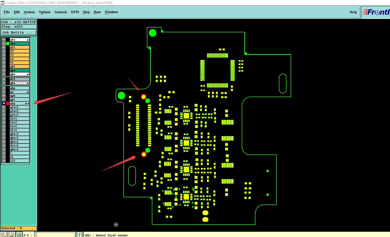
Figure 1: more openings in solder paste layer
Risk indicators included the dense pad population that left almost no free real estate for legend enlargement, the aluminum-plugged via process that further constrained surface features, the very short three-day lead time, and the small overall board size. On such a compact 6-layer PCB design any illegible marking quickly becomes a yield or acceptance problem.
| Feature Observed | Condition in Files | Primary DFM Risk |
|---|---|---|
| Silkscreen character size | Below 0.1 mm width / 0.7 mm height | Blurred or incomplete legend |
| Paste vs solder-mask openings | Inconsistent at several locations | Potential tinning or registration issues |
| MARK point openings | Paste and mask mismatch | Fiducial recognition risk |
Table 1 summarizes the key observations that generated the Engineering Question.
Silkscreen Minimum Size and Opening Mismatch Risks Identified
The dominant risk was silkscreen characters smaller than the process capability of 0.1 mm width and 0.7 mm height. When characters are this small the screen-printing process cannot resolve clean edges; the result is blurred, broken, or incomplete text after curing. A second risk involved inconsistencies between the solder-paste layer openings and the solder-mask openings. Because the production files followed the original solder mask geometry, any paste-layer deviation could produce incorrect tinning areas or registration problems at MARK points. A third observation concerned the complete lack of free space to enlarge or move the undersized characters due to the dense pad layout and aluminum-plugged vias.
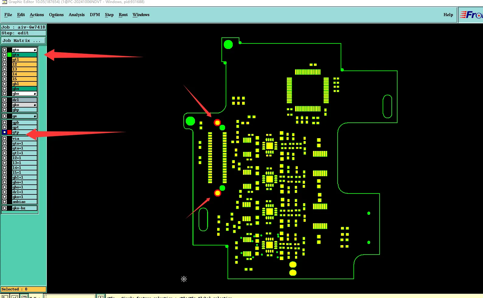
Figure 2: the solder paste layer and the solder mask layer are inconsistent
From a DFM perspective the priority sequence was clear: obtain explicit customer acceptance of possible blur for the undersized legend, clarify whether the paste-layer openings should be forced to match the solder-mask openings, and confirm the MARK-point treatment before any tooling was released under the three-day schedule.
How Undersized Silkscreen Compromises Legibility and Yield
If production had continued without addressing the Silkscreen Minimum Size violation, the finished boards would have carried blurred or incomplete white characters on the green solder-mask surface. Based on IPC-A-600 acceptability considerations, illegible legend is frequently classified as a process indicator or minor defect that can still trigger customer rejection, especially on prototype or low-volume lots where visual quality is closely scrutinized. Blurred markings also reduce the ability to identify boards in the field or during rework, creating traceability problems.
The paste-to-mask opening mismatch introduced a parallel risk. If the stencil openings differed from the solder-mask openings, the amount of solder paste deposited could be incorrect, leading to insufficient or excessive solder on critical pads. At MARK points the mismatch could impair automated optical recognition during assembly, causing placement errors or machine stops. On a board with aluminum-plugged vias the surface topography is already more complex; any additional registration or tinning variation increases the chance of cosmetic or functional defects.
Because the board is only 66 mm by 75 mm and packed with pads, there was simply no free real estate to enlarge the characters. Attempting to force larger text would have caused the legend to overlap copper or mask openings, creating new solderability or shorting risks. Acceptance of possible blur, or an updated silkscreen file, therefore became the only practical paths forward.
| Potential Failure Mode | Root Cause Linked to EQ | Production or Field Impact |
|---|---|---|
| Blurred or incomplete legend | Characters below 0.1 / 0.7 mm | Cosmetic rejects, lost traceability |
| Incorrect solder volume | Paste vs mask opening mismatch | Weak joints or bridging at assembly |
| Fiducial recognition failure | MARK point paste/mask inconsistency | Placement errors, machine stops |
| Legend overlap on copper | No space to enlarge characters | Solderability defects if forced |
Table 2 maps each realistic failure mode to the Engineering Question items.
Failure Scenarios the Engineering Team Sought to Prevent
Had the undersized characters been printed without confirmation, the boards would have left the factory with blurred or broken white text. On a five-piece prototype lot such cosmetic defects often trigger full rejection, forcing a complete respin under the already tight three-day window. Even if the boards were accepted, field technicians would struggle to read part numbers or reference designators, increasing the risk of incorrect rework or misidentification.
Leaving the paste-to-mask opening mismatch unresolved could have produced incorrect solder-paste volumes on critical pads or impaired MARK-point recognition during automated assembly. Either outcome would have generated placement defects or machine stops that are expensive to correct on a small, dense board. Forcing larger characters into the limited free space would have caused the legend to overlap copper or mask openings, creating new solderability problems that are worse than simple blur.
All of these scenarios share a common origin: insufficient design-for-manufacturing margin at the silkscreen and opening interfaces on a pad-dense 6-layer board.
Preventive Actions Confirmed During the DFM Exchange
Our engineering team issued a clear Engineering Question that first addressed the Silkscreen Minimum Size issue. Because the characters measured below the process capability of 0.1 mm width and 0.7 mm height, and because the dense pad layout left no free space for enlargement or relocation, the team recommended that the customer either accept possible blur or supply an updated silkscreen file with larger characters. The production files were prepared according to suggestion 1 (process-limited printing with acceptance of blur) unless the customer replied that the files were in error and required a new legend upload.
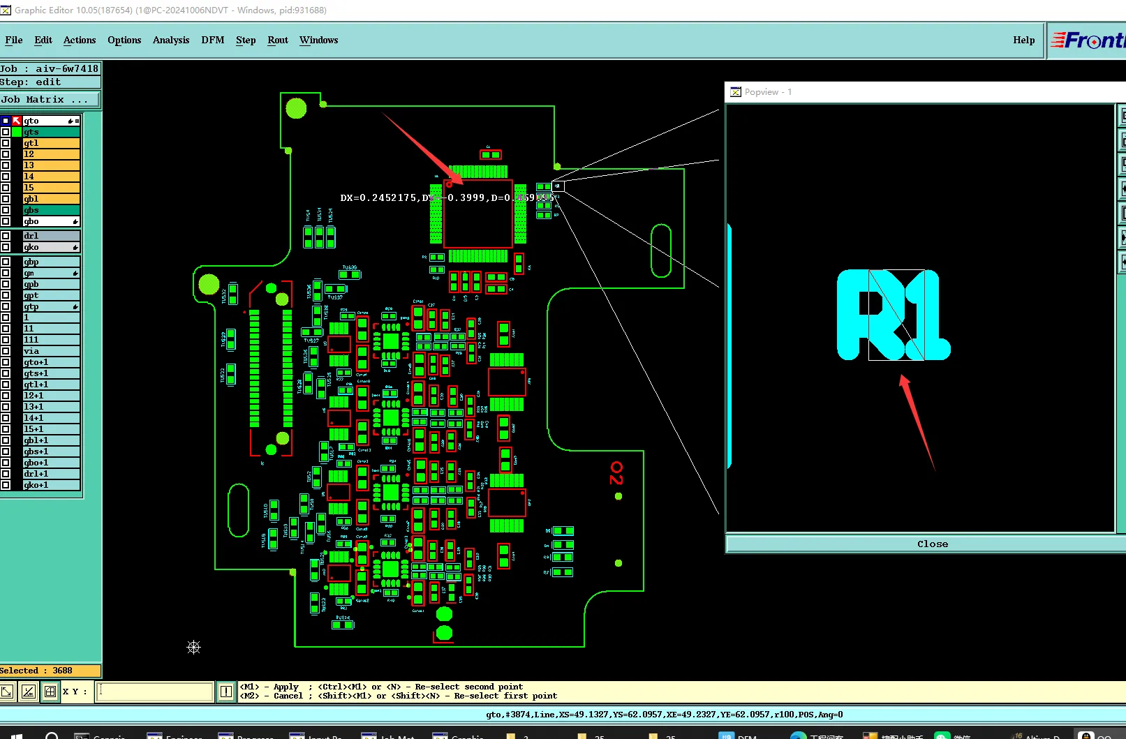
Figure 3: the text is too small to make
For the paste-to-mask opening mismatch the team noted that production files followed the original solder-mask geometry. The customer was asked to confirm whether the paste-layer openings should be forced to match the mask openings for proper tinning, especially at MARK points. The same confirmation was requested for the MARK-point openings themselves.
With customer acknowledgment of the process limits and the handling of the opening inconsistencies, the CAM data were finalized and the order released under the three-day schedule. The revised approach retained all electrical functionality while documenting the expected legend appearance and ensuring consistent surface openings.
| Action Item | Customer Decision Direction | Manufacturing Benefit |
|---|---|---|
| Silkscreen character size | Accept blur or supply updated file | Clear process limit, no forced overlap |
| Paste vs mask openings | Follow original solder-mask geometry | Consistent tinning and registration |
| MARK point openings | Confirmed treatment | Reliable fiducial recognition |
Table 3 records the closed-loop decisions that converted a high-risk legend design into a manufacturable product.
Building Trust Through Early Legend and Opening Verification
This case demonstrates that Silkscreen Minimum Size is not a minor cosmetic detail on dense 6-layer boards; it is a direct determinant of visual quality, traceability, and customer acceptance. By identifying characters below the 0.1 mm / 0.7 mm process limit during CAM review and obtaining explicit customer direction on blur versus file update, the engineering team protected both first-pass yield and the three-day delivery commitment. Clarification of the paste-to-mask and MARK-point openings further reduced the chance of assembly-side registration or tinning problems.
Designers working with pad-dense multilayer boards are encouraged to keep silkscreen characters above the practical minimum size, reserve clear space for legend enlargement when pads are numerous, align paste-layer openings with solder-mask openings, and request early DFM feedback on legend feasibility. These practices convert potential manufacturing and cosmetic problems into controlled, documented decisions before production begins.
Proactive verification of Silkscreen Minimum Size remains one of the highest-leverage actions a DFM team can take when releasing compact, high-density multilayer boards.
FAQ
Q1: Why does silkscreen character size have a practical minimum of approximately 0.1 mm width and 0.7 mm height?
A1: Screen-printing resolution and ink flow limit the ability to form clean edges below these dimensions. Characters smaller than the process capability tend to print blurred, broken, or incomplete after curing.
Q2: What happens if undersized silkscreen is printed without customer confirmation?
A2: The legend appears blurred or incomplete, triggering cosmetic rejects under IPC-A-600 visual criteria and reducing field traceability. On small prototype lots such defects often force a full respin.
Q3: Why is free space critical when silkscreen characters are too small?
A3: Enlarging or relocating characters requires clear area free of copper and mask openings. On dense pad boards that space does not exist, so the only practical options are acceptance of blur or an updated legend file.
Q4: How does a paste-to-solder-mask opening mismatch affect assembly?
A4: Incorrect stencil openings can deposit the wrong volume of solder paste, leading to weak joints or bridging. At MARK points the mismatch can impair automated fiducial recognition and cause placement errors.
Q5: Can blurred silkscreen still be electrically acceptable?
A5: Yes. The legend is non-functional, so electrical performance is unaffected. However, cosmetic rejection and loss of traceability remain real risks that must be accepted or corrected by the customer.
Q6: How can designers avoid similar Silkscreen Minimum Size issues on future dense boards?
A6: Keep characters above the practical minimum size (approximately 0.1 mm width / 0.7 mm height), reserve clear space for legend when pads are numerous, align paste-layer openings with solder-mask openings, and request early DFM review of legend feasibility. These steps form the practical foundation of reliable silkscreen design on high-density multilayer boards.