When a PCB impedance package reaches CAM, the fabrication note, impedance table, stackup, and Gerber do not always describe the same geometry. The note may list a target, layer, trace width, and pair spacing, while the Gerber on that layer is missing the listed geometry, contains a nearby differential pair, or uses one width for two different impedance targets.
That mismatch is what this review addresses. The question is not whether the board "needs impedance." The question is which impedance instruction is actually tied to the released copper, and what has to be confirmed before CAM can release the geometry for fabrication.
The cases below are examples from recent packages, not a complete list of every way an impedance table and copper file can fall out of alignment.
| What we saw in the files | Where the files disagree | What the EQ asked |
|---|---|---|
| Note lists 5/5 mil 90 ohm traces; a 5/5.1 mil differential pair is on the layer | No 5/5 mil traces in the copper; a near-geometry pair is there | Point to the 5/5 mil 90 ohm nets, or accept the 5/5.1 mil pair as that row |
| Inner-layer 90 ohm released at 4.16/7 mil; a figure shows 7/4.16 mil | Artwork is still 4.16/7 mil; the swap changes both width and pair spacing | Keep 4.16/7 mil, or accept 7/4.16 mil as the inner 90 ohm row |
| One trace width asked to meet 100 ohm differential and 50 ohm single-ended | Two targets sit on one geometry; the EQ calculation does not close both | Keep both targets with a new width, spacing, or stackup, or control 100 ohm differential only |
PCB Impedance Control in the Released Note and Gerber
In a released package, PCB stackup impedance control is split between the requirement and the copper geometry. The note or table says what the line is supposed to be — 90 ohm, 100 ohm differential, 50 ohm single-ended — and on which layer, at which trace width, and at which pair spacing if it is a differential pair. The copper file is what was actually drawn. CAM is reading the gap between those two sources.
Some packages put the row in fabrication notes. Some put it on a drawing impedance table. A stackup drawing may repeat the same numbers. Net names in CAD only help when the note already points at them. A net label by itself does not invent a missing width.
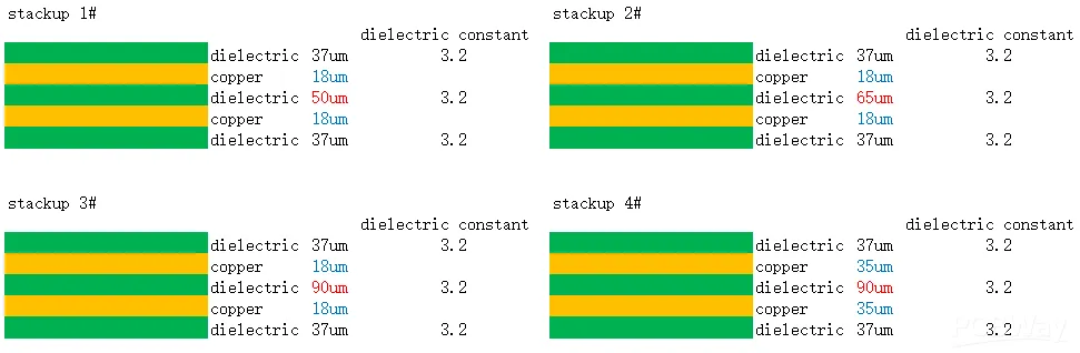
A stackup drawing with no traces on it also does not identify the 90 ohm set or the 100 ohm differential pair. Dielectric thickness and copper thickness on that drawing are inputs that were already in the package. If a later press figure changes the core or prepreg, that change belongs in the stackup review unless the same figure is explicitly tied to a revised impedance row. Until then we list every table line, see whether copper exists on the named layer, and flag any second source that already moves width, spacing, or construction.
PCB Trace Impedance Versus Trace Width and Differential Pair Spacing
Laying the table on the copper answers a narrow question: what geometry was released? We can measure trace width on the named layer and spacing on a candidate differential pair. We can say pair or single. We can say the measured width and spacing are exact, close, or simply not there against the table row. That identifies the released geometry. It does not establish the impedance the etched line will achieve.
So 5/5.1 mil does not become the 5/5 mil 90 ohm row just because the numbers look similar. 4.16/7 mil does not become 7/4.16 mil as a drawing typo. One width does not automatically carry both differential impedance and single-ended impedance. Width and pair spacing are separate inputs. A differential pair uses both. A single-ended row uses width against the reference dielectric.
A 5/5.1 mil differential pair is on the layer
The stackup used for the EQ calculation has to be the one identified in that calculation. If the proposed impedance change comes with a revised stackup, that construction has to be confirmed with the impedance close. This review does not publish a field-solver result, a dielectric constant, an etch factor, or a tolerance band as a factory default. Coupon artwork and the traveler follow the width and spacing named in the close. They do not follow a table row that has no copper under it.
| What the note and the copper show | What still has to be confirmed |
|---|---|
| Every table row: target ohms, single-ended or differential, layer, width, pair spacing | Which document owns the row when a later figure already changes width, spacing, or construction |
| Measured trace width on the named layer, and spacing of a candidate differential pair | Whether a 0.1 mil near-geometry pair is that row, or a different set of traces |
| Pair versus single on the flashed copper | Whether one width is being asked to carry both a differential target and a single-ended target |
| Exact, near, or absent against the table width and spacing | Whether a proposed width/spacing swap is accepted as new copper, not as a label edit |
| The ohms the note assigned to that geometry | The ohms the etched line will actually hold — that number is not a CAM measurement |
90 Ohm Trace Impedance Listed at 5/5 mil When the File Shows a Differential Pair
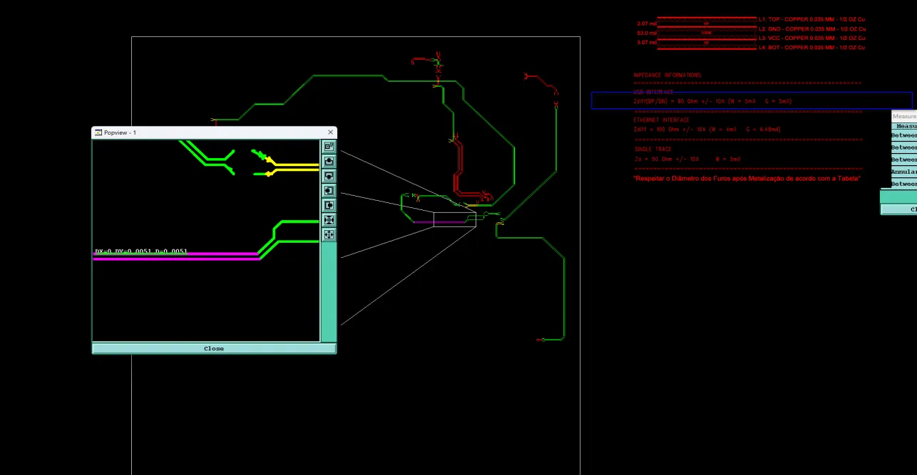
On one package the notes listed 5/5 mil 90 ohm impedance traces. Those traces were not in the file. A 5/5.1 mil differential pair was on the same layer. We looked for 5/5 mil singles and pairs and did not find them. The 5/5.1 mil pair is what the artwork released.
A 5/5 mil 90 ohm row with no copper behind it is not something the shop can put on a traveler. The 5/5.1 mil pair is a different row. The 0.1 mil difference is an identification miss, not a capability argument and not an automatic stand-in. Coupon and traveler follow the width and spacing that get agreed. They cannot be loaded from a table line that never made it into the Gerber.
The files themselves do not pick a reading. The 5/5.1 mil pair may be the 90 ohm set and the table may be stale. The 5/5 mil 90 ohm set may never have been routed. Both may have been intended and only one drawn. We measure the 5/5.1 mil pair only to identify it, then ask the customer to point at the 90 ohm nets or to accept that pair as the row.
Impedance Trace Width and Spacing on an Inner-Layer 90 Ohm Pair
Another package called inner-layer 90 ohm. The released geometry was 4.16 mil width and 7 mil spacing. The EQ came back with a figure that moved impedance trace width and spacing to 7/4.16 mil and asked whether that was acceptable. This kind of change highlights why a careful DFM review for impedance control is important when validating PCB geometry.
Until that figure is accepted, the artwork is still 4.16/7 mil. Moving to 7/4.16 mil changes both numbers. That is a new pair, not a cleaned-up label. Differential impedance on that inner pair uses width and spacing together; they are not interchangeable.
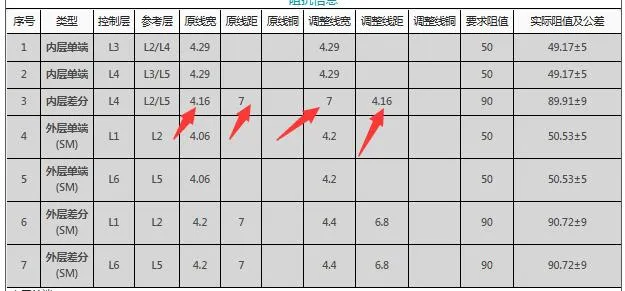
The line width/space needs to be adjusted from 4.16/7 mil to 7/4.16 mil
The reason the EQ appears is simple enough to state without printing the math: on the released stackup, the original width and spacing do not land on the 90 ohm target in the factory calculation. Taking the swap changes inner copper, not only the table text. Leaving the artwork alone keeps 4.16/7 mil and leaves the 90 ohm row open unless the target or the stackup moves instead.
If the same figure also changes core, prepreg, or ounce, that construction piece is confirmed with the impedance close. If the press figure is still in dispute after that, it goes to stackup review. The impedance row and the press figure are not rewritten off each other in the background.
100 Ohm Differential Impedance and 50 Ohm Single-Ended on One Trace Width
A third package asked one impedance trace width to meet 100 ohm differential impedance and 50 ohm single-ended. The calculation attached to the EQ did not close both. The factory proposed to control only 100 ohm differential and to attach an impedance and stackup figure. This is a typical impedance conflict that needs to be resolved against the actual PCB construction rather than treated as a labeling issue.
Those are two different rows. They are not the same structure at one width on one dielectric. Differential impedance of the pair depends on width and spacing. Single-ended impedance of one of those traces depends on width and the reference dielectric. The conflict is two fabrication limits written onto one geometry. It is not an impedance-matching or termination problem.
The proposal — control 100 ohm differential only, see the attached impedance and stackup adjustment — drops the 50 ohm single-ended limit. That is a named close on that job, not a shop default and not a standard 50/100 ohm construction. If the customer does not take it, both targets stay, and width, spacing, or stackup has to change until they sit on separate rows. The other way is to keep the artwork and rewrite the table to one target.
On the EQ we split the request into two table lines, show the released one-width combination as the conflict, and stay on the attached figure. The question is which target remains a control limit, and whether that stackup figure is accepted with it.
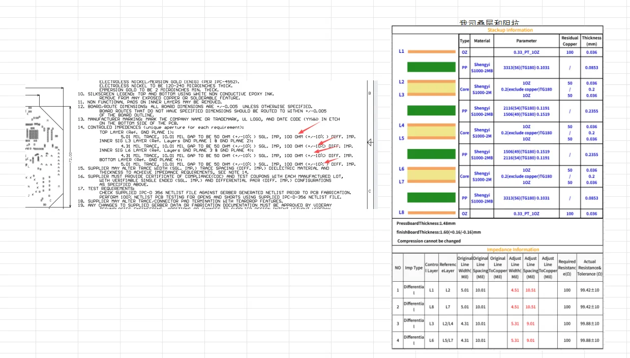
The recommended stackup and trace width adjustment
Keep the Released PCB Impedance Table or Confirm the Trace Width
Each row needs a written answer. Mixed answers are fine: accept the 5/5.1 mil pair as the 90 ohm row and keep 4.16/7 mil on the inner pair; drop the 50 ohm single-ended limit and leave every other row as drawn. A partial close still has to name the revised table line and the revised Gerber width. Anything it leaves unnamed stays as released.
The three paths already sit in the EQs.
Keep the released table and copper. The customer points to the missing 5/5 mil 90 ohm nets, or keeps 4.16/7 mil and both the 100 ohm and 50 ohm targets. CAM does not substitute 5/5.1 mil, swap width and spacing, or drop 50 ohm on its own.
Accept the identified or retuned geometry. The 5/5.1 mil differential pair becomes the 90 ohm row, or inner 90 ohm moves to 7/4.16 mil. The table and the traveler follow the accepted trace width and spacing.
Accept one control limit and the attached stackup figure. The dual-target width is rewritten to 100 ohm differential only. 50 ohm single-ended is no longer a fabrication control. Construction on that figure is confirmed in the same close.
None of those paths invents a tolerance, a coupon spec, or a standard 50/100 ohm factory default.
| Released conflict | What CAM can show | Close that needs a name on it |
|---|---|---|
| 5/5 mil 90 ohm listed; 5/5.1 mil pair in the file | No 5/5 mil traces; a near-geometry differential pair exists | Point to the 5/5 mil nets, or accept 5/5.1 mil as that row |
| Inner 90 ohm at 4.16/7 mil; figure shows 7/4.16 mil | Artwork still 4.16/7 mil; the swap is a new trace width and spacing | Keep 4.16/7 mil, or accept 7/4.16 mil |
| One width for 100 ohm differential and 50 ohm single-ended | Two targets on one geometry; the EQ says both do not close | Keep both targets with a new width/spacing or stackup, or control 100 ohm differential only |
After that answer, one table owns the job: target, single-ended or differential, layer, trace width, and pair spacing. Copper on the named layer either stays as released or shows the agreed width and spacing.
Before the package goes out, put the impedance table next to the copper on the named layers. If a row is missing, near, swapped, or carrying two targets, write the chosen path into the note. That missing line is how this kind of EQ starts. Until it is written, the released table and the released trace width stay as drawn.
FAQ
Q1: What is PCB trace impedance?
A1: The ohms the note assigned to a released width on a named layer. CAM can measure that width, and pair spacing if it is a differential pair. That tells us which geometry was drawn. It does not produce the ohms on the etched line.
Q2: What is the difference between single-ended impedance and differential impedance?
A2: Single-ended impedance is one trace against its reference dielectric. Differential impedance is a pair and uses both width and spacing. Writing both targets onto one width is how the 100 ohm / 50 ohm EQ starts.
Q3: What is a PCB differential pair?
A3: Two traces on the same layer whose width and spacing belong to one differential-impedance row. Measuring one width without the spacing does not identify that row.
Q4: What trace width is used for PCB impedance control?
A4: Whatever width the table named and the copper actually flashed. Pair spacing is a separate number when the row is differential. A 5/5.1 mil pair is not the 5/5 mil row. Moving 4.16/7 mil to 7/4.16 mil changes both numbers and waits on the close.
Q5: What is PCB impedance matching?
A5: PCB impedance matching generally refers to designing and controlling transmission-line impedance so that the interconnect meets the intended electrical requirement. In CAM review, the practical issue is often more basic: the impedance target, stackup, and released trace geometry must describe the same construction.
Q6: Can one PCB trace width be 100 ohm differential and 50 ohm single-ended?
A6: On the example job the attached calculation did not close both on the released width. The factory offered to control only 100 ohm differential and to attach an impedance and stackup figure. Keeping both targets means changing width, spacing, or stackup until they are separate rows, or rewriting the table to one target.
Q7: Who decides the impedance table versus the Gerber trace width?
A7: The customer, in a written close that names the row, the accepted width and spacing, and any stackup figure that came with that row. CAM records exact, near, or absent. Until that line is written, the released table and the released copper stay as drawn.