4-layer boards with 3mil line/space and impedance requirements often surface multiple DFM conflicts during CAM review. This real engineering case reviews a 4-layer FR-4 design that required extensive clarification before production. As a senior CAM engineer with 15+ years of experience, I regularly see how tight feature sizes combined with copper weight and impedance demands create significant manufacturing risks if not addressed early.
This project highlighted the gap between customer design intent and actual factory process capabilities. Below I detail the key issues we identified, the reasoning behind our engineering questions, and how we resolved them to protect yield and reliability.
Order Overview
This was a 4-layer FR-4 PCB( #FR4-20260106-056 ) using TG150 material from KB, finished thickness 1.6mm, with 1oz copper on all layers. Minimum line/space was 3mil, minimum hole size 0.2mm. Surface finish was ENIG, with green solder mask and white silkscreen. The design included impedance control and required 100% flying probe testing. Panelization was 1x1 with V-cut capability. Quantity was 10 pieces (10 sets).
While the base parameters appeared standard for a mid-complexity digital board, the combination of fine 3mil features, impedance requirements, and specific hole treatments triggered several critical engineering concerns during our standard CAM data review.
Main Engineering Questions Found During CAM Review
Outer Copper Thickness vs Fine Line/Space Capability
The customer specified finished outer copper thickness of 35um ±10%, but with 3/3mil line/space and 1oz base copper, this target conflicted with our etching process capabilities. We noticed this discrepancy while analyzing the fine features.
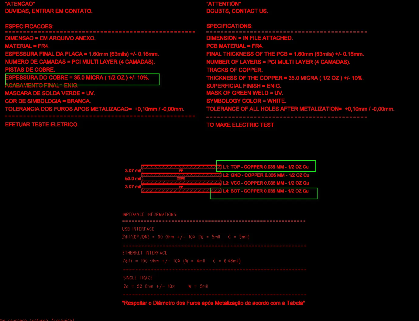
Figure 1: customer specified finished outer copper thickness of 35um ±10%
Our engineer recommended confirming a more realistic copper thickness because attempting to maintain 35um ±10% on such fine lines would cause severe undercutting and open circuits. If ignored, the production run could result in significant yield loss, with many traces either over-etched (open) or under-etched (shorts). We have seen similar cases lead to complete scrap of panels.
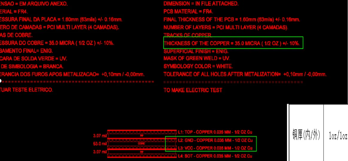
Figure 2: the inner copper thickness requirements are not consistent
The customer eventually accepted adjustment to standard 1oz finished weight to ensure reliable etching.
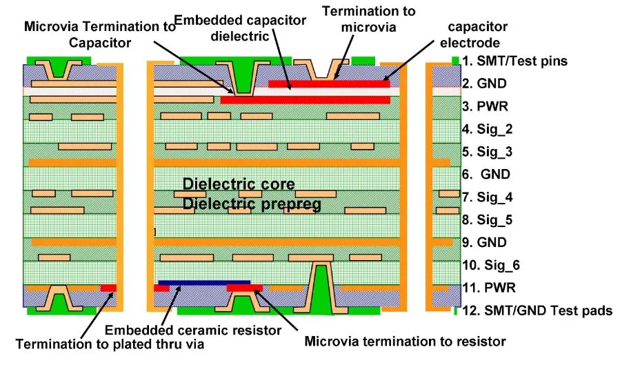
Impedance Control and Stackup Adjustment Request
The stackup file and impedance requirements were provided, but several reference traces (including 5/5mil 90ohm lines) could not be located in the actual Gerber data. Instead, we found 5/5.1mil differential pairs. We also proposed adjusting trace widths/spaces and stackup to achieve the target impedance based on our actual material performance.
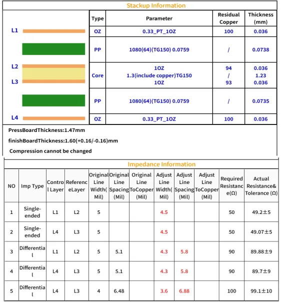
Figure 3: stackup file and impedance requirements
After reviewing the stackup, we found that strict adherence to the original data would make consistent impedance difficult. According to IPC-2221 guidelines, proper modeling and adjustment are essential for controlled impedance boards. Proceeding without confirmation risked boards failing signal integrity requirements, leading to costly respins or field failures due to reflections and timing issues.
We requested permission to optimize trace geometry and stackup, which the customer approved after review.
Solder Mask Bridge on Tight 3mil Features
Several pad-to-pad spacings were only 5mil. After compensation, our standard green solder mask process could not guarantee reliable bridges. For 1oz copper, we typically require minimum 7.5mil spacing to ensure mask bridges.
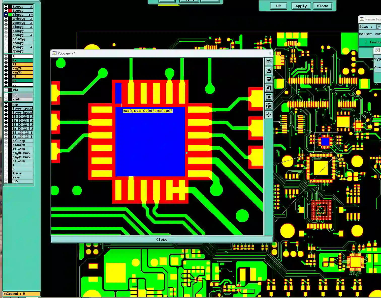
Figure 4: pad-to-pad spacings were only 5mil
We noticed this during solder mask data analysis. If ignored, the boards could suffer from mask voids or solder bridging during assembly, causing shorts or poor solderability. In high-volume production this often leads to assembly failures and rework. We confirmed acceptance of no-bridge conditions in those areas.
Hole Treatment and Mask Opening Issues
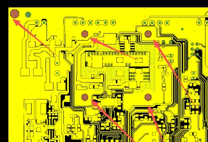
Multiple holes were defined as PTH but had no annular ring or electrical connection. Some 1.0mm holes lacked mask openings on both sides, which would allow solder mask ink to enter the holes. We also identified inconsistent drill tolerances and inner copper thickness specifications.
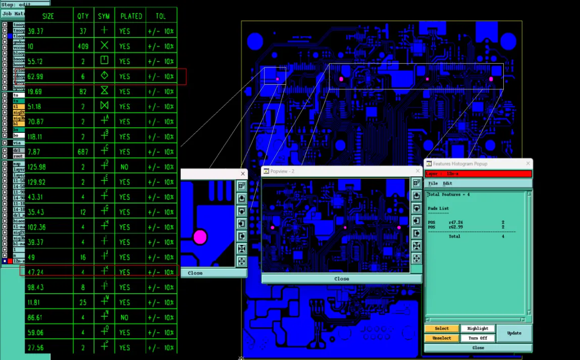
Figure 5: PTH but had no annular ring or electrical connection
Figure 6: some 1.0mm holes lacked mask openings on both sides
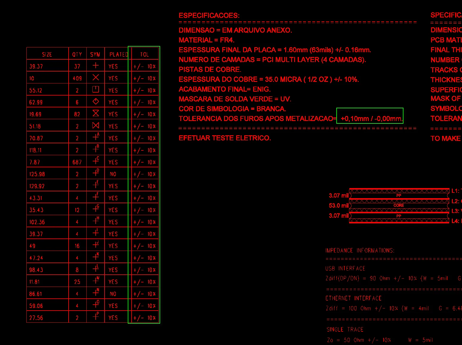
Figure 7: inconsistent drill tolerances and inner copper thickness specifications
Our CAM team flagged these for confirmation because incorrect hole plating or ink-filled vias can cause open circuits or assembly problems. The customer clarified which holes should be non-plated.
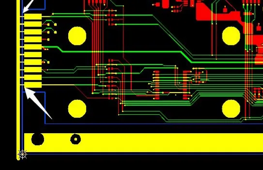
Process Edge and Silkscreen Concerns
The process edge lacked tool holes and fiducials. Some silkscreen characters overlapped or were too close to pads. These were resolved with standard confirmations and minor adjustments.
Figure 8: Some silkscreen characters overlapped or were too close to pads
Figure 9: adding tool holes and fiducials
Manufacturing Risks and DFM Insights
This case clearly demonstrates common pitfalls in fine-line 4-layer designs: over-specified copper thickness on tight features, incomplete impedance reference data, and optimistic solder mask bridge expectations. These issues frequently cause EQs because they directly impact etching, impedance consistency, and assembly yield.
If left unaddressed, such problems often result in open/short circuits, impedance deviation, solder mask defects, and high scrap rates. In past similar orders, unconfirmed copper thickness led to severe undercutting and over 40% yield loss.
How the Engineering Team Resolved the Issues
Our team prepared detailed markup files highlighting each concern. For copper thickness and impedance, we provided calculated alternatives and received approval to optimize within manufacturable limits. Solder mask bridge areas were reviewed with the customer, who accepted no-bridge conditions where necessary.
We noticed the conflicting hole definitions early and clarified plating requirements case by case. All production files were updated after customer confirmations, significantly reducing manufacturing risk.
Final Manufacturing Outcome
All engineering questions were resolved through customer feedback. Production data was adjusted for realistic copper thickness, optimized impedance geometry, confirmed hole treatments, and accepted solder mask parameters. The order was approved and released for manufacturing.
Key Takeaways for PCB Designers
- Verify that all impedance reference traces are clearly present and match the specified values in your Gerber files.
- Balance copper thickness specifications with your minimum line/space requirements — finer features usually need thinner finished copper.
- Check solder mask bridge capability against your fabricator's design rules before releasing tight pad spacings.
- Clearly define PTH versus NPTH holes, especially when annular rings are minimal or absent.
- Include tool holes and fiducials on process edges for accurate panelization and registration.
- Keep silkscreen features away from pads to prevent soldering issues.
- Provide complete, consistent stackup drawings and allow reasonable manufacturing adjustments for impedance.
FAQ
Q1: Why is copper thickness critical for 3mil line/space designs?
A1: Thicker copper requires more etching time, which increases the risk of undercutting and trace width reduction on fine features, potentially causing opens or impedance shifts.
Q2: What happens if impedance reference traces are missing?
A2: The factory cannot accurately model or verify impedance, often requiring adjustments to trace geometry or stackup to meet targets.
Q3: Can solder mask bridges always be guaranteed on 5mil pad spacing?
A3: Not with standard green mask and 1oz copper. Most factories need 7-8mil spacing for reliable bridges to avoid voids or bridging during assembly.
Q4: Why do factories request stackup adjustments for impedance?
A4: Actual material dielectric constants and press parameters may differ slightly from the design file, requiring minor optimizations to achieve target impedance values consistently.
Q5: Should designers always add tool holes on process edges?
A5: Yes. They improve panel registration, alignment during drilling and routing, and overall manufacturing accuracy.