










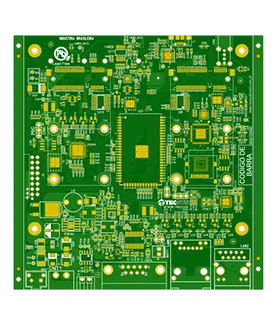
PCB Specifications
| Parameter | Value | Parameter | Value |
|---|---|---|---|
| PCB Type | FR4 PCB | Quantity | 10 pcs |
| Layers | 4 Layers | Board Type | Panel PCB |
| Dimensions | 120 x 122 mm | Copper Weight | 1oz |
| Thickness | 1.6 mm | Min Track / Spacing | 3/3mil |
| Surface Finish | ENIG (Immersion Gold) | Min Hole Size | 0.2mm |
| Solder Mask | Green | Silkscreen | White |
| Stack-up | Default | Impedance Control | Yes |
Manufacturing Timeline
Logistics Information
Key Manufacturing Processes
Manufacturing Summary
This 4-layer FR-4 board (120 × 122 mm, 1.6 mm finished thickness, TG150 KB-6165F material) was produced as single-unit panels for a quantity of 10 pieces. It featured 1 oz copper on all layers, 3 mil minimum line/space, 0.2 mm minimum hole size, green solder mask, white legend, and ENIG surface finish. The order required impedance control and 100% flying probe testing with V-scoring for final separation. The tight geometries and controlled impedance made this a fine-line multilayer build.
DFM review highlighted several specification conflicts that needed resolution. Requested impedance lines of 5/5 mil for 90 ohms were not located in the files; we identified actual differential pairs and adjusted trace widths and stackup to meet the target impedance. Outer copper thickness requirements (35 ±10% µm) conflicted with the fine 3/3 mil geometries and standard 1 oz foil, so we confirmed achievable values. Solder mask bridge capability was limited on 5 mil pad spacings with 1 oz copper; we clarified acceptance criteria for potential bridge loss. Additional issues addressed included inconsistent drill tolerances, PTH hole definitions on non-connected equal-size pads, missing process tooling holes, character placement near pads, and solder mask opening on specific vias. impedance control and solder mask bridge handling were managed through customer-confirmed adjustments and file revisions.
All engineering questions were resolved prior to production release. The order completed within the 10-day delivery window using mechanical forming. Final electrical testing and quality documentation confirmed compliance with the adjusted parameters and controlled processes.
Explore More PCB Manufacturing Resources
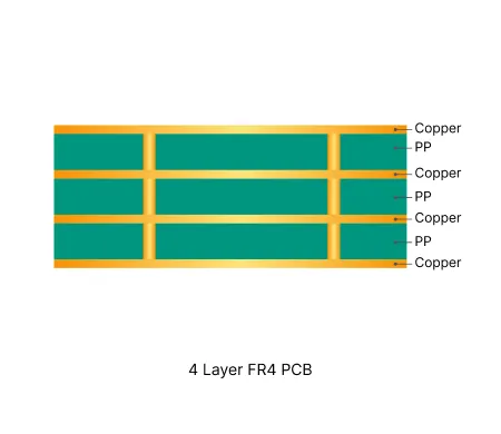
4 Layer FR4 PCB Manufacturing Insights
Standard multilayer solution offering practical routing density and controlled impedance for industrial and consumer electronics.

Multilayer FR4 PCB Engineering Queries Explained: Causes, Risks and Solutions
In-depth guide to the most frequent Engineering Queries (EQ) and DFM issues in Multilayer FR4 PCB (4/6/8+ layers) production. Real factory insights on stack-up confirmation, impedance control, copper balance, inner layer design, via treatment, registration, and practical prevention strategies.
Real Production Records
| Order ID | PCB Type | Layers | Dimensions | Solder Mask | Surface Finish | Quantity | Action |
|---|---|---|---|---|---|---|---|
| FR4-20260918-083 | FR4 PCB | 4 | 98 x 25 | Green | HASL Lead Free | 10 | View detail |
| FR4-20260918-033 | FR4 PCB | 6 | 55 x 41.7 | Green | ENIG (Immersion Gold) | 5 | View detail |
| FR4-20260912-059 | FR4 PCB | 2 | 275 x 193.7 | Green | ENIG (Immersion Gold) | 100 | View detail |


