










In a 6-layer FR4 order (192.53 × 149.86 mm, 1.6mm thickness, 15 pieces, TG170 material, 0.5oz/1oz copper with ENIG finish), the working files presented several critical DFM concerns. The design included specific impedance requirements (90 ohm inner layer and 50 ohm on L4) and a non-standard stackup, triggering detailed engineering review before production could begin.
Non-Standard Stackup and Its Impact on Impedance
During initial 6-layer FR4 PCB ( #FR4-20260519-059 ) CAM analysis, our engineer noted that the customer-specified stackup deviated from our standard configurations for 6-layer builds. This immediately raised concerns about manufacturability and the ability to consistently achieve the required impedance values. The files were re-submitted with adjustments, but confirmation was essential to align the physical layer construction with both design intent and production capabilities.
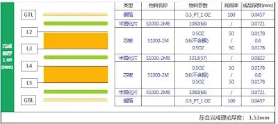
Figure 1: our standard configurations for 6-layer builds
Impedance control is highly sensitive to dielectric thickness, copper weight, and layer ordering. A non-standard stackup increases the risk of deviation in actual electrical performance once the board is laminated and etched.
Inner Layer Line Width Adjustment for 90 Ohm Impedance
The original data proposed inner layer traces at 4.16 mil width with 7 mil spacing for the 90 ohm requirement. Upon review, our engineering team identified that these dimensions were marginal for reliable etching on 0.5oz copper within our standard process parameters. Further analysis showed that reversing the dimensions to 7 mil width and 4.16 mil spacing would better align with the target impedance while staying within controllable manufacturing tolerances.
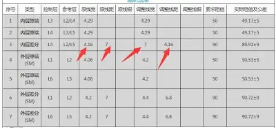
Figure 2: the line width/space needs to be adjusted from 4.16/7 mil to 7/4.16 mil
This adjustment was not arbitrary. Etching narrower traces (4.16 mil) on thinner copper carries higher risk of over-etching, necking, or inconsistent width, which directly impacts impedance tolerance. The recommended change provides more robust process margin without significantly altering the overall design intent. During the EQ process, we explained the reasoning based on our historical data for similar 6-layer controlled impedance builds, and the customer agreed to the modification in the updated files.
From a DFM perspective, such fine-tuning early in the review prevents downstream issues like trace open circuits or impedance drift that could only be discovered after fabrication and electrical testing.
Copper Pour Deficiency Affecting 50 Ohm Impedance on L4
A notable concern was the 50 ohm impedance region on Layer 4, where the design lacked adequate copper pour for reference plane shielding. Without a continuous or sufficiently dense ground/power plane in proximity, the impedance calculation becomes unreliable. Our engineer flagged this after cross-checking the impedance callout against the actual copper distribution in the Gerber files.
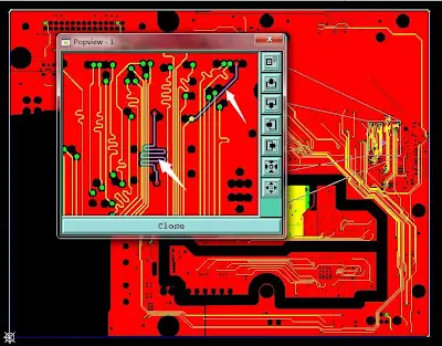
Figure 3: the indicated area requires 50-ohm impedance
In multi-layer impedance designs, a solid reference plane is essential for maintaining consistent characteristic impedance and minimizing crosstalk or EMI. The absence of copper in this area would likely cause the actual impedance to deviate significantly from the 50 ohm target, potentially leading to signal reflections, reduced noise margin, or failure in functional testing. We recommended adding appropriate copper pour or stitching to create a proper reference, while respecting any clearance requirements around sensitive traces.
This issue highlighted the importance of verifying not just trace geometry but also the surrounding copper environment when impedance is specified. The customer confirmed the need for this adjustment in the revised files.
| Impedance Requirement | Original Design | Recommended Adjustment | Risk if Unchanged |
|---|---|---|---|
| Inner Layer 90 Ohm | 4.16/7 mil | 7/4.16 mil | Etching variation |
| L4 50 Ohm Area | No copper pour | Add reference plane | Inaccurate impedance |
Table 1: Impedance-Related DFM Adjustments. The table illustrates the key changes proposed to achieve stable electrical performance in this 6-layer construction.
Missing Solder Mask Openings on Critical Holes
Two holes were identified in the design with no solder mask openings defined on either side. With green solder mask and ENIG surface finish specified, this created a clear risk of solder mask ink flowing into or fully covering the hole entrances during the printing process. For a 6-layer board with 0.2mm minimum drill size, proper mask clearance is important for reliable plating and to prevent contamination during subsequent finishing steps.

Figure 4: no solder mask opening on the top or bottom side
Our review confirmed that these holes were intended as functional features (likely vias or component holes). Without openings, there is a high probability of mask residue remaining inside the holes after development, which could interfere with ENIG plating uniformity or cause probe contact issues during 100% flying probe testing. In production, this has been known to result in intermittent electrical failures or reduced long-term reliability due to trapped residues.
We recommended adding appropriate solder mask openings with standard clearance to ensure clean hole walls and good plating quality. The customer confirmed this change, resolving the potential defect source before lamination began.
How These Issues Threatened Final Board Performance
From a reliability standpoint, using a non-standard stackup without confirmation could lead to inconsistent dielectric spacing and copper thickness after lamination, directly affecting impedance tolerance. According to IPC-6012 standards, controlled impedance designs require precise layer registration and material control.
Incorrect trace widths or missing reference planes often result in signal integrity problems, such as reflections or crosstalk, that only become apparent during testing or in the end application. Missing solder mask openings risk ink contamination in holes, leading to plating defects or assembly issues.
Potential Failure Scenarios the Team Aimed to Avoid
If the stackup and impedance adjustments had been ignored, the finished boards could exhibit impedance values outside the target range, causing signal distortion or timing issues in high-speed applications. In the worst case, this leads to functional failures after assembly.
Without solder mask openings, ink could enter the holes, resulting in blocked or poorly plated features and potential open circuits or poor ENIG coverage. The missing copper pour on L4 would likely produce unreliable 50 ohm performance, risking product qualification failure or field reliability problems.
Engineering Recommendations and Customer Confirmation Process
Our DFM team recommended adopting the standard AIVON 6-layer stackup for better process control and proposed the trace width swap for the 90 ohm lines. We also advised adding copper pour on L4 for proper reference and confirming solder mask openings on the identified holes. Markings for UL and date code were reviewed for position accuracy.
The customer provided updated files and confirmations, allowing production to proceed with high confidence. These changes ensured the 4-day turnaround remained feasible while mitigating key risks.
| Concern | Recommendation | Outcome |
|---|---|---|
| Stackup | Use standard configuration | Improved consistency |
| Impedance Traces | Width/spacing swap | Better etching control |
| Solder Mask & Copper Pour | Add openings and pour | Reliable plating and impedance |
Table 2: Key DFM Resolutions. These adjustments transformed potential production risks into a manufacturable design.
Value of Proactive DFM in Controlled Impedance Designs
This 6-layer case demonstrates how early identification of stackup, impedance, and mask-related issues prevents costly surprises. By addressing these during review, we protected both short-term yield and long-term product reliability. Designers working on impedance-sensitive boards benefit greatly from involving DFM expertise before finalizing files.
FAQ
Q1: Why is stackup confirmation critical for multi-layer impedance designs?
A1: Non-standard stackups can cause variations in dielectric thickness and layer registration, leading to impedance values outside specification and potential signal integrity failures.
Q2: How does trace width adjustment affect impedance control?
A2: Optimal width and spacing depend on the chosen stackup and copper weight. Incorrect dimensions often result in etching inconsistencies and out-of-tolerance impedance.
Q3: What risks arise from missing solder mask openings on holes?
A3: Solder mask ink can enter or block holes, causing plating defects, contamination, or poor ENIG coverage that leads to assembly or reliability issues.
Q4: Why does a 50 ohm area need proper copper pour on reference layers?
A4: Without shielding copper, the impedance calculation becomes inaccurate due to lack of a consistent reference plane, resulting in performance that deviates from design targets.
Q5: When should impedance-sensitive designs undergo DFM review?
A5: As early as possible, ideally before finalizing trace geometries and stackup. Early review prevents multiple revision cycles and ensures the board performs as intended.






