8-layer impedance controlled designs frequently require detailed DFM clarification during CAM review. This engineering case examines a real 8-layer FR-4 board that presented several critical manufacturability issues. As a senior CAM engineer with over 15 years of experience, I often see how conflicting electrical requirements and mechanical specifications create production risks if not resolved before fabrication.
This project involved tight 4mil line/space, dual impedance targets, and large mechanical features. The article details the key engineering questions we raised, the manufacturing limitations involved, and how we worked with the customer to ensure a successful outcome.
Order Overview
This was an 8-layer FR-4 PCB ( #FR4-20260422-008 ) using TG170 material with a finished thickness of 1.6mm and 1oz copper on all layers. Minimum hole size was 0.3mm with 4mil line/space. Surface finish was ENIG, with matte black solder mask and white silkscreen. The design required impedance control with a report, 100% flying probe testing, and V-cut panelization. Quantity was 5 pieces (5 sets).
While the board size (195x114mm) and layer count were standard for networking or industrial applications, the combination of dual impedance requirements, large slots/holes, and specific tolerance notes triggered multiple engineering concerns during our standard CAM review process.
Main Engineering Questions Found During CAM Review
Impedance Control Conflict: Differential vs Single-Ended Requirements
The most critical issue was the impedance specification. The customer required the same trace width to meet both 100ohm differential and 50ohm single-ended impedance. After calculation using our actual material parameters, we found this combination impossible to achieve simultaneously.
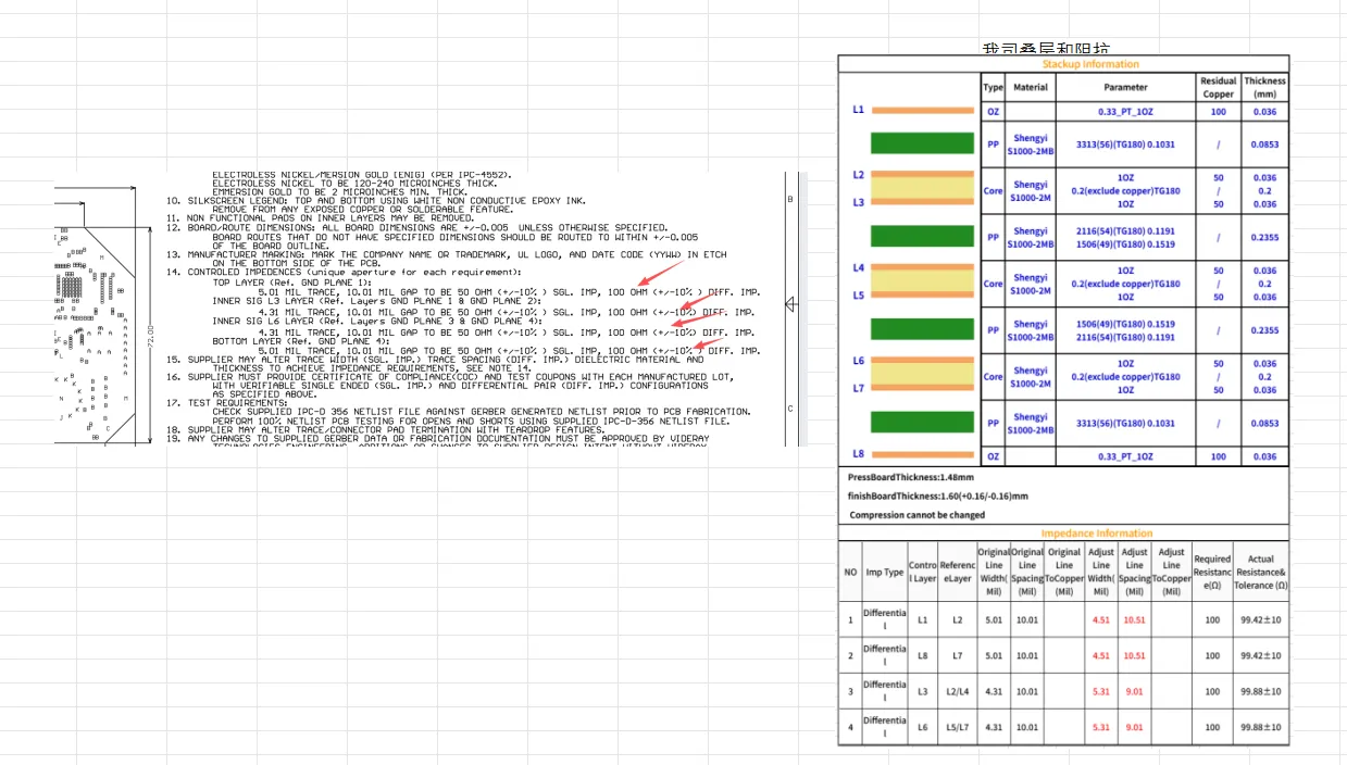
Figure 1: recommended stackup and trace width adjustment
Our engineer suggested controlling only the 100ohm differential impedance and provided a recommended stackup and trace width adjustment. We noticed this during detailed impedance modeling. According to common IPC-2221 practices for controlled impedance, conflicting targets on the same geometry often require design trade-offs. If ignored, the boards would likely fail impedance testing, resulting in signal instability, reflections, or complete functional failure in high-speed applications.
The customer reviewed our proposed stackup adjustment and approved the change to prioritize differential impedance.
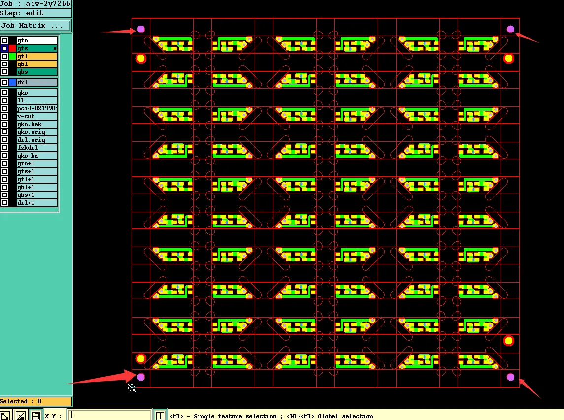
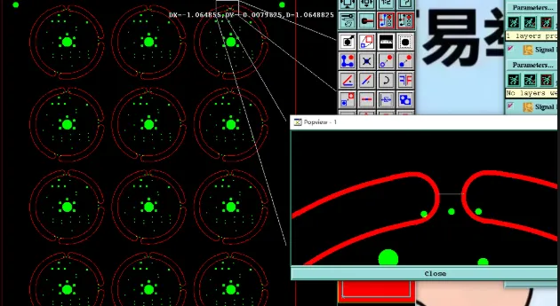
Large Hole and Slot Dimension Tolerances
Three slots and three large holes exceeded our drilling capability in length and diameter. We recommended relaxing the tolerance to ±0.1mm and routing them during the shaping process instead of drilling.
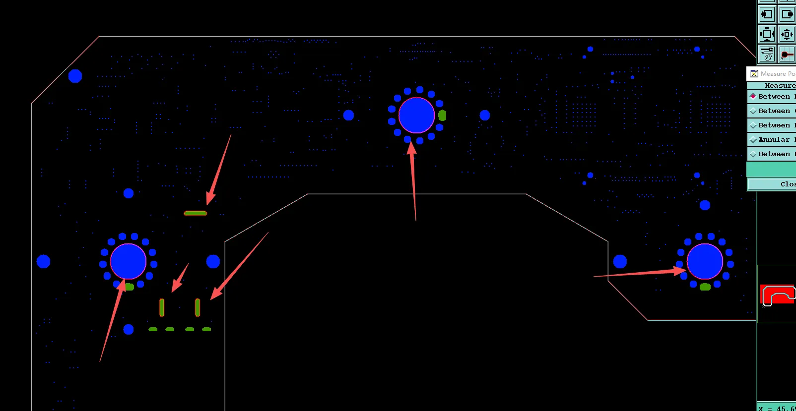
Figure 2: three slots and three large holes are too long or too large in diameter
We identified this during mechanical data review. If production continued without adjustment, it could cause drill breakage, irregular hole shapes, or significant dimensional deviation. In extreme cases, this leads to scrap boards or assembly misalignment. The customer accepted the tolerance relaxation after reviewing our proposal.
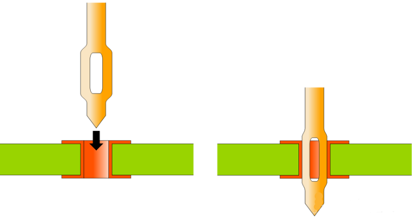
Outer Copper Thickness and Stackup Consistency
The stackup drawing showed inconsistent copper thickness compared to the order specification. We confirmed production using finished 1oz outer copper weight as per the order details.
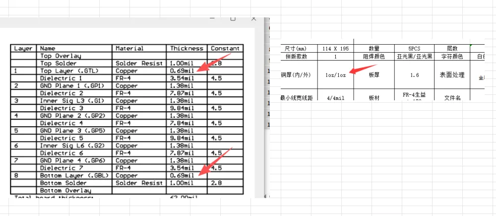
Figure 3: inconsistent copper thickness compared to the order specification
After reviewing the stackup, we found this mismatch could affect etching uniformity and impedance accuracy. Proceeding with conflicting data risked copper peeling or trace width deviation. We clarified and aligned to the order specification.
Solder Mask Thickness and IPC Netlist Issues
The specified solder mask thickness was too stringent. We suggested our standard 8-30um range. Additionally, the IPC netlist showed opens and shorts, and the latest production files had network deviations, leading us to recommend ignoring the netlist check.
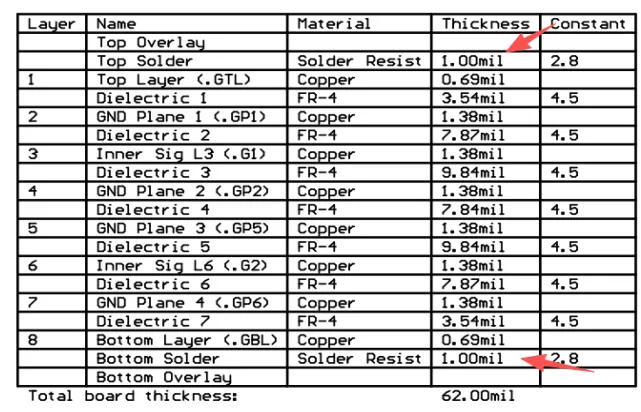
Figure 4: specified solder mask thickness was too stringent
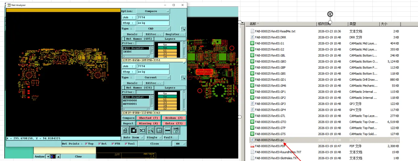
Figure 5: the IPC netlist showed opens and shorts
These issues, while less structural, can still impact final quality. The customer accepted standard mask thickness and netlist handling.
Manufacturing Risks and DFM Insights
This case highlights recurring challenges in 8-layer designs: conflicting impedance targets on shared geometries, oversized mechanical features, and documentation inconsistencies. Designers often set aggressive dual impedance requirements without considering actual dielectric performance, and mechanical tolerances that exceed standard drilling limits.
If ignored, these issues commonly cause impedance test failures, drill-related defects, etching problems, and yield reduction. In similar past projects, unaddressed impedance conflicts resulted in full lot rejection after electrical testing.
How the Engineering Team Resolved the Issues
Our CAM team provided detailed markup drawings and calculation reports for the impedance adjustment. We suggested and received approval for stackup optimization to meet the primary 100ohm differential requirement. For the large holes and slots, we proposed routing with relaxed tolerance, which was accepted.
We noticed the copper thickness mismatch early and aligned all data to the order specification. Panelization was confirmed as compatible, and standard processes were applied for solder mask and netlist handling. This structured clarification prevented multiple revision cycles.
Final Manufacturing Outcome
All engineering questions were resolved with customer approval. Production files were updated with optimized impedance parameters, adjusted mechanical tolerances, confirmed copper thickness, and standard process controls. The order was successfully released for fabrication.
Key Takeaways for PCB Designers
- Verify that dual impedance requirements (differential + single-ended) are physically achievable on the same trace geometry before finalizing the design.
- Provide clear mechanical tolerance expectations for large holes and slots, considering drilling vs routing limitations.
- Ensure stackup drawings and order specifications are fully consistent regarding copper weights and thicknesses.
- Allow reasonable manufacturing adjustments to impedance lines and stackup when targeting tight tolerances.
- Design large cutouts and slots with practical tolerances to avoid tool limitations on multilayer boards.
- Confirm IPC netlist usage and provide the most up-to-date production files for accurate checking.
- Specify realistic solder mask thickness requirements based on standard factory capabilities.
FAQ
Q1: Why is it often impossible to meet both differential and single-ended impedance with the same trace width?
A1: Differential and single-ended impedance have different geometry dependencies. Achieving both simultaneously usually requires different trace widths or adjusted spacing, necessitating design trade-offs.
Q2: What risks arise from oversized holes and slots in multilayer PCBs?
A2: Standard drilling may fail, causing tool breakage, irregular dimensions, or delamination. Routing with relaxed tolerance is often safer for large features.
Q3: Why do factories request copper thickness clarification?
A3: Inconsistencies between stackup drawings and order specs can lead to etching problems, impedance deviation, or plating issues if not aligned early.
Q4: Should designers always allow impedance adjustments during CAM review?
A4: Yes, especially when material performance differs slightly from theoretical values. Minor adjustments often ensure the board meets the primary impedance targets reliably.
Q5: What is the impact of overly tight solder mask thickness requirements?
A5: It can cause inconsistent coverage or process instability. Standard ranges (8-30um) usually provide better reliability without compromising performance.