PCB Specifications
| Parameter | Value | Parameter | Value |
|---|---|---|---|
| PCB Type | FR4 PCB | Quantity | 50 pcs |
| Layers | 2 Layers | Board Type | Panel PCB |
| Dimensions | 310 x 310 mm | Copper Weight | 1oz |
| Thickness | 1 mm | Min Track / Spacing | 5/5mil |
| Surface Finish | HASL Lead Free | Min Hole Size | 0.3mm↑ |
| Solder Mask | Green | Silkscreen | White |
| Stack-up | Custom | Impedance Control | No |
Manufacturing Timeline
Logistics Information
Key Manufacturing Processes
Manufacturing Summary
This 2-layer FR-4 board measured 310 × 310 mm with 1 oz copper on both sides and a 1.0 mm finished thickness using KB-6165F TG150 material. Produced in a quantity of 50 pieces as customer self-panelized single units with V-cut and routing separation and no process edges, the design featured 5 mil line/space, 0.3 mm holes, and lead-free HASL surface finish. 100% flying probe testing was completed for this large-panel, short-turnaround order.
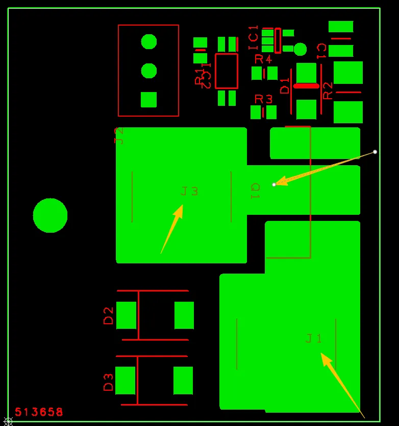
DFM review addressed several layout concerns. Multiple holes showed asymmetric copper pads on one side only, requiring confirmation of plated versus non-plated attributes. Copper features and traces approached the board outline too closely, risking exposure, burrs, and lifting after routing or V-cut. Silkscreen characters placed on the outline layer were relocated to the proper top layer, while undersized etching text was enlarged to the minimum 6 mil for reliable readability. Via tenting specifications were clarified for consistency with customer notes. Fiducials and mark points were added to process areas per standard practice after confirmation.
The order completed successfully within 2 days with all boards meeting electrical and dimensional requirements. The large square panels maintained flatness and registration throughout processing despite the absence of dedicated process edges.
Explore More PCB Manufacturing Resources
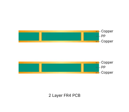
2 Layer FR4 PCB Manufacturing Insights
2 layer FR4 PCBs deliver cost-effective solutions for most electronic designs. Their simple structure enables consistent quality and efficient production cycles.
Common Engineering Queries in 2 Layer FR4 PCB Design and Manufacturing
Real Engineering Queries (EQ) and DFM issues for 2 Layer FR4 PCB (double-sided boards) from actual production reviews. Learn how to avoid common problems with via treatment, silkscreen on pads, solder mask openings, hole attributes, board edge clearance, and other frequent design pitfalls.
Real Production Records
| Order ID | PCB Type | Layers | Dimensions | Solder Mask | Surface Finish | Quantity | Action |
|---|---|---|---|---|---|---|---|
| FR4-20260528-028 | FR4 PCB | 2 | 185 x 245 | Green | HASL Lead Free | 5 | View detail |
| FR4-20260526-001 | FR4 PCB | 2 | 100 x 100 | Green | HASL Lead Free | 10 | View detail |
| FR4-20260525-001 | FR4 PCB | 2 | 50 x 45 | Matte Green | HASL Lead Free | 20 | View detail |


