In high-mix PCB production, even well-intentioned customer designs often encounter manufacturability gaps during CAM engineering review. This 8-layer FR-4 board (#FR4-20260110-007) with TG170 material, 0.8mm finished thickness, and mixed 2oz/1oz copper weights presented several classic DFM conflicts that required immediate clarification before panelization and lamination.
Our CAM team identified issues ranging from inner layer copper spacing constraints to panelization details and solder mask inconsistencies. These are common in dense multilayer boards where design intent meets real factory process capabilities. Early EQ resolution prevented potential scrap, yield loss, and production delays.
Order Overview
This was a standard 8-layer build using FR-4 base material with TG170 rating, targeting a finished board thickness of 0.8mm. Outer layers specified 2oz copper while inner layers were initially called out at 2oz, creating immediate spacing concerns given the 4mil minimum trace/space in the provided data. The board featured ENIG surface finish, 0.1mm minimum hole size, 100% flying probe testing, and no blind vias or buried vias noted in the primary stackup.
Panelization was set for 3x5 array on a single panel with stamp holes and bridge connections. Total quantity was 225pcs (15 sets), with mechanical routing and specific process edge requirements. The design included green solder mask on both sides and white silkscreen limited to the top layer. Delivery was requested within 14 days.
Such configurations are typical for industrial control or consumer electronics applications but frequently trigger engineering questions due to the balance required between electrical performance (thicker copper) and fabrication reliability (etching and registration tolerances).
Main Engineering Questions Found During CAM Review
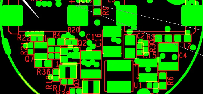
1. Inner Layer Copper Weight Conflict with Minimum Spacing
The most critical issue was the customer's requirement for 2oz copper on inner layers combined with 4mil trace/space. Our CAM engineer identified this during initial data analysis. After review by our senior engineering lead, we determined that maintaining 2oz inner copper would violate standard etching capabilities for reliable yield at this geometry.
![]()
Figure 1: Customer's requirement for 2oz copper on inner layers combined with 4mil trace/space
We noticed the inner layer copper thickness specification directly conflicted with the provided Gerber data. To reduce manufacturing risk, our engineer recommended changing inner layers to 1oz copper while keeping outer layers at 2oz. If ignored, this could lead to over-etching, trace necking, open circuits, or severe undercutting that compromises impedance control and structural integrity.
Figure 2: Changing inner layers to 1oz copper while keeping outer layers at 2oz
According to typical IPC-2221 guidelines for copper weight and conductor spacing, the 2oz configuration at 4mil approached or exceeded safe limits for standard FR-4 processing, especially with the required registration tolerances on an 8-layer board. Changing to 1oz inner copper resolved the etching window while preserving overall electrical performance.
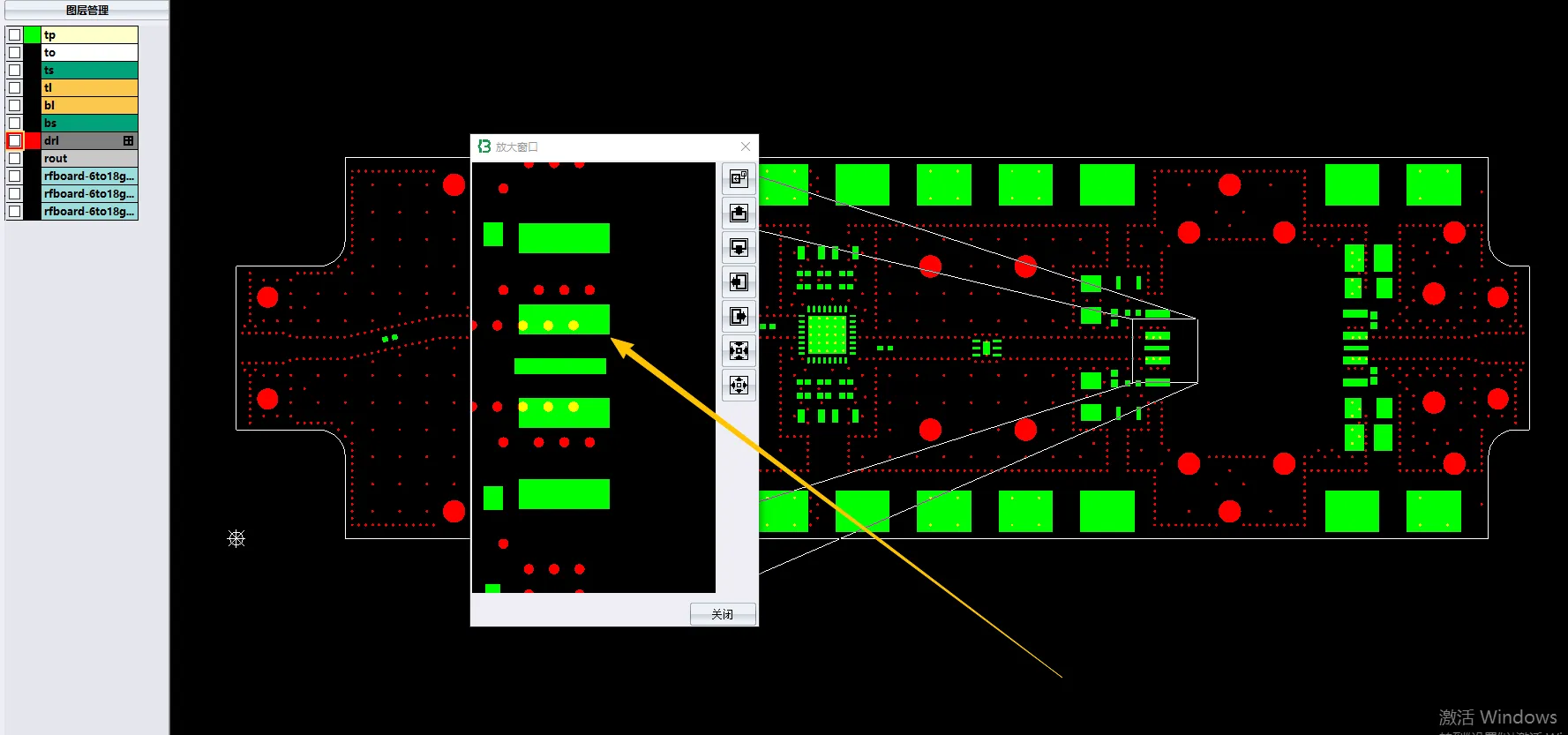
2. Panelization and Process Edge Optimization
The customer provided initial panelization data, but our team optimized it to a straight + bridge + stamp hole configuration for better stability during routing and depanelization. We attached the optimized panel drawing and asked for confirmation.
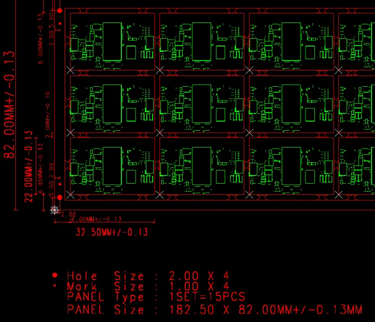
Figure 3: Optimized panel drawing
Our engineer suggested adjusting the copper clearance because we noticed the V-CUT area (process edge 4mm) was too close to exposed copper features in the original layout. If the V-CUT clearance had not been adjusted, exposed copper could appear after depanelization, potentially causing edge shorting during assembly or reliability issues in the field due to oxidation and contamination.
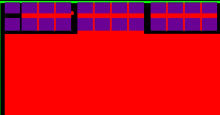
Additionally, multiple pads were found with insufficient distance (less than 0.2mm) to the board edge. The finished board would likely show exposed copper after routing, violating IPC-A-600 acceptability criteria and risking cosmetic defects or assembly problems.
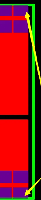
Figure 4: Multiple pads with insufficient distance (less than 0.2mm) to the board edge
3. Solder Mask and Silkscreen Data Inconsistencies
Review of the bottom layer solder mask revealed conflicts with the steel mesh (stencil) data. The bottom solder mask opening showed only specific traces indicated by arrows, which did not match the overall design intent. We requested customer confirmation on the intended solder mask pattern.

Figure 5: Bottom solder mask opening showed only specific traces indicated by arrows.
We also clarified that our production would apply white silkscreen only on the top layer as per standard practice for this order.

Figure 6: White silkscreen only on the top layer
Open window areas showing both copper exposure and substrate exposure required explicit confirmation to avoid unintended mask coverage or clearance issues that could affect solderability.
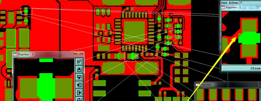
Figure 7: Open window areas showing both copper exposure and substrate exposure.
4. Board Thickness and Lamination Parameters
Two areas in the fabrication notes specified conflicting board thickness requirements. Our team proposed an optimized lamination stackup with inner layers at 1oz copper, targeting 0.89mm finished thickness (±0.1mm tolerance). This adjustment aligned with material availability and press parameters for TG170 FR-4.
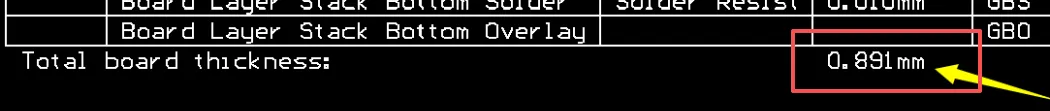
Figure 8: 0.89mm finished thickness
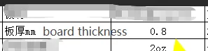
Figure 9: Board thickness in the fabrication notes
If the inconsistent thickness calls had been ignored, it could result in out-of-spec boards leading to assembly fit issues, impedance deviation, or even delamination under thermal stress.
Suggested EQ Categories
File & Manufacturing Data Issues
- Solder mask vs. stencil data mismatch on bottom layer
- Inconsistent board thickness notes in fabrication drawing
- Silkscreen layer scope (top layer only)
Stackup & Material Issues
- Inner layer 2oz copper vs. 4mil spacing manufacturability
- Optimized lamination for target 0.89mm thickness
Panelization & Process Optimization
- Optimized 3x5 panel with stamp holes and bridges
- Process edge copper clearance for V-CUT/routing
- Pad-to-edge clearance verification
Solder Mask & Silkscreen Issues
- Open window confirmation for exposed copper/substrate areas
Manufacturing Risks and DFM Insights
This case highlights several recurring DFM pitfalls in multilayer PCB orders. The copper weight versus spacing conflict is particularly common when designers prioritize current-carrying capacity without verifying etching tolerances. Ignoring it risks trace width reduction beyond acceptable limits per IPC-6012, leading to high scrap rates and signal integrity problems.
Edge clearance violations often cause cosmetic failures or functional shorts after depanelization. In high-volume runs like 225pcs, even a 5-10% yield loss from exposed copper or breakout can significantly impact project timelines and costs.
Panelization details matter immensely for mechanical stability. Poor stamp hole or bridge placement can cause board vibration during routing, resulting in resin voids, copper peeling, or registration errors across layers.
Our CAM review workflow caught these before production, avoiding multiple revision cycles that commonly delay projects by 3-7 days.
How the Engineering Team Resolved the Issues
Our team worked quickly to provide optimized files. For the copper weight issue, we confirmed the change to 1oz inner layers with the customer and updated the stackup accordingly. The lamination parameters were adjusted to achieve 0.89mm nominal thickness, providing a safe tolerance window.
We shared the revised panelization diagram showing clear stamp holes and bridge connections. Edge clearance adjustments were proposed where feasible, with confirmation on acceptable exposed copper windows. Solder mask and silkscreen clarifications ensured alignment between design files and production output.
Throughout the process, we maintained transparent communication, providing marked-up images for each point. This collaborative approach is standard in our factory to protect both yield and customer satisfaction.
Final Manufacturing Outcome
All engineering questions were resolved with customer approval. The stackup was optimized, panelization approved, and data files updated. The order was released for production with confirmed parameters: inner copper at 1oz, target thickness 0.89mm ±0.1mm, and verified clearances. CAM review was completed successfully, and boards proceeded to fabrication.
Key Takeaways for PCB Designers
- Always verify copper weight against minimum trace/space in your Gerber data before release. Thicker copper requires proportionally larger clearances.
- Provide clear layer stackup drawings with exact copper weights per layer and expected finished thickness tolerances.
- Include sufficient copper-to-edge clearance (typically ≥0.2-0.3mm after routing) in your design to prevent post-depanelization exposure issues.
- Ensure solder mask and stencil data are consistent and clearly documented. Mismatches trigger unnecessary back-and-forth.
- Use standard naming conventions for layers and include fabrication notes in a dedicated drawing rather than scattered across files.
- Consider panelization early. Share your preferred array and allow the factory to propose optimizations for better manufacturability.
- Specify silkscreen requirements explicitly (top only, bottom only, or both) to avoid assumptions.
- Request a pre-production DFM review if your design includes tight tolerances or mixed copper weights.
FAQ
Q1: Why must inner layer copper weight sometimes be reduced from 2oz to 1oz?
A1: At fine geometries like 4mil trace/space, 2oz copper significantly narrows the etching process window, increasing risks of shorts, opens, or inconsistent trace widths. Reducing to 1oz maintains design functionality while ensuring reliable yield.
Q2: What happens if pad-to-board-edge clearance is insufficient?
A2: After mechanical routing or V-CUT, copper can become exposed on the edge, leading to potential shorts, oxidation, or assembly defects. This often fails IPC-A-600 visual acceptance criteria.
Q3: Why do factories optimize panelization with stamp holes and bridges?
A3: Proper panelization improves mechanical stability during processing, reduces vibration-induced defects, and ensures clean depanelization without damaging individual boards.
Q4: How important is solder mask data consistency with other files?
A4: Inconsistent mask data can cause incomplete coverage or unwanted openings, affecting solderability, electrical isolation, and long-term reliability. CAM engineers always verify alignment.
Q5: Can board thickness notes be inconsistent in fabrication drawings?
A5: No. Conflicting thickness requirements create ambiguity in lamination and final inspection. Factories must clarify to guarantee the board meets both mechanical and electrical specifications.
Q6: What is the benefit of early EQ communication during CAM review?
A6: It prevents production of non-conforming boards, reduces scrap costs, shortens overall lead time, and builds a smoother collaboration between designer and manufacturer.