Panelized multilayer PCBs with V-cut and routing combinations often surface multiple DFM issues during CAM review. This engineering case examines order(#FR4-20260113-031) — a 4-layer FR-4 design sized 130 × 130 mm, 1.2 mm finished thickness, with customer-provided 3×3 panelization. During our standard CAM engineering review, several critical discrepancies emerged regarding stackup construction, depanelization details, fiducial protection, and marking placement.
As a senior CAM engineer, I've handled hundreds of similar jobs where customer panelization intent conflicts with actual manufacturing constraints. These issues, if left unaddressed, can lead to severe production problems. Our team raised targeted EQs to align the data with factory capabilities before releasing for production.
Order Overview
This 4-layer PCB used FR-4 TG170 material with a finished thickness of 1.2 mm. Outer copper was 1 oz, inner layers 1.5 oz. Minimum hole diameter was 0.25 mm, surface finish ENIG. The board was panelized by the customer in 3×3 array with V-cut plus routing for depanelization. Quantity was 135 pcs (15 sets). 100% flying probe testing was required. The design featured green solder mask, white silkscreen, and mechanical forming. While the parameters looked standard, the combination of thin 1.2 mm thickness, customer panelization, and specific marking requirements triggered detailed engineering scrutiny.
Main Engineering Questions Found During CAM Review
Stackup Construction and Core Material Adjustment
After reviewing the customer's stackup reference, we found that our standard stocked cores are copper-clad. We noticed a mismatch with the expected copper-free core assumption in the provided diagram. Our engineer suggested adjusting the lamination parameters based on actual available material to maintain the target 1.2 mm finished thickness.
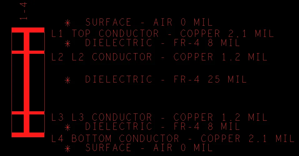
Figure 1: Stackup reference
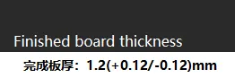
Figure 2: Finished board thickness
If this adjustment had not been confirmed, the final board thickness could deviate significantly, leading to potential warpage in such a thin 1.2 mm construction or impedance variation if controlled. In extreme cases, mismatched dielectric thickness can cause delamination under thermal stress during assembly.
Panelization, Depanelization, and Fiducial Protection
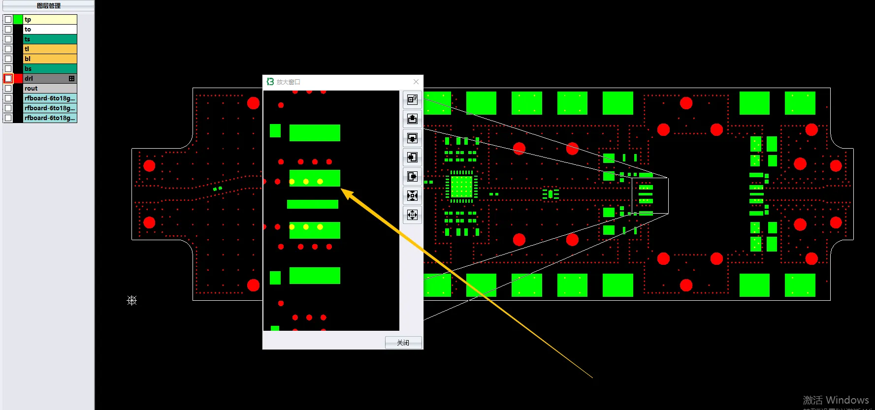
The customer's 3×3 panelization with V-cut and routing required careful review. We identified that stamp holes on the side farther from the PCS could cause premature breaking during handling. Our team recommended canceling those distant stamp holes to ensure clean depanelization from the correct side.
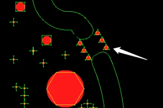
Figure 3: Stamp holes on the side farther from the PCS
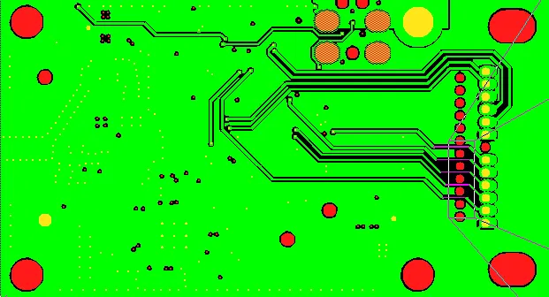
Additionally, we noticed the optical fiducials on the process edge were at risk of falling off during production. To reduce manufacturing risk, our engineer suggested adding a protective copper ring around these fiducials. Without this protection, fiducial loss could disrupt automated assembly alignment, resulting in placement errors and high scrap rates.
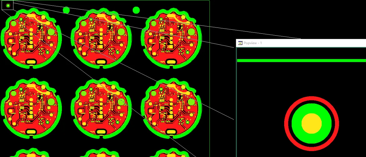
Figure 4: Adding a protective copper ring around optical fiducials
Special Optical Features and Unknown Pad Structures
We noticed several optical points in the design files and asked the customer to confirm whether these needed to be added to every individual PCS. In the upper left corner, there was a large pad with solder mask opening and silkscreen of identical size but no corresponding drill hole. Our CAM team could not clearly identify its specific function or purpose.
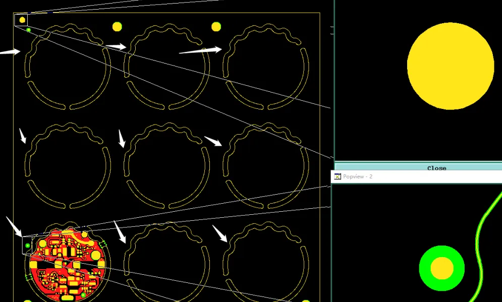
Figure 5: A large pad with solder mask opening in the upper left corner
This kind of ambiguous feature is common in customer-supplied data. If left unconfirmed, it could lead to unnecessary processing steps, potential short circuits from unplated large copper features, or cosmetic inconsistencies. We required clarification to decide whether to replicate the feature across all boards or treat it as a panel-level marker only.
Marking Placement: UL, Serial Numbers, and Silkscreen
Several marking issues arose. The customer requested UL marking on the top layer, while the order specified bottom. Given our expired UL certification at the time, we recommended omitting it to avoid compliance complications. Due to the small PCS size and solder mask openings, there was insufficient space for production serial numbers or UL on the board itself. We suggested placing them on the process edge instead.
![]()
Figure 6: UL marking requirement
Silkscreen elements overlapping solder mask openings were adjusted by our team to prevent printing on pads. If ignored, this could cause poor solderability or cosmetic defects failing IPC-A-600 standards.
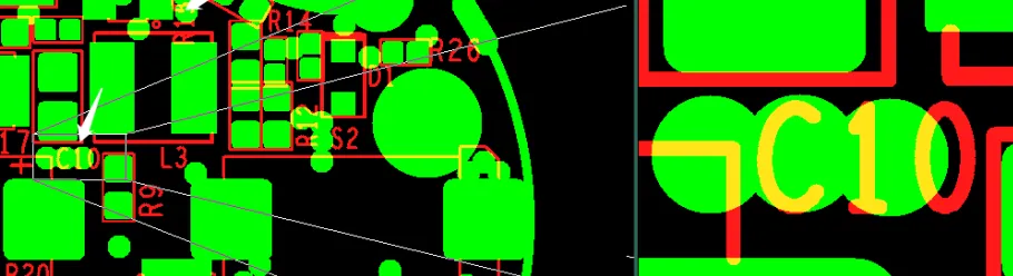
Figure 7: Silkscreen elements overlapping solder mask openings
Suggested EQ Categories
Stackup & Material Issues
- Copper-clad core adjustment for 1.2 mm thickness
- Lamination parameter confirmation
Panelization & Process Optimization
- Stamp hole placement for controlled depanelization
- Fiducial protection ring on process edge
- V-cut + routing interaction
File & Manufacturing Data Issues
- UL marking layer conflict and feasibility
- Production serial number placement on small boards
- Silkscreen adjustment over solder mask openings
Manufacturing Risks and DFM Insights
Thin 1.2 mm panels with customer-defined 3×3 arrays are prone to handling and depanelization problems. Incorrect stamp hole positioning can cause boards to separate prematurely, leading to edge damage or misalignment in downstream processes. Without protective rings, process edge fiducials are vulnerable to mechanical abrasion, directly impacting SMT line performance.
Marking placement conflicts are common when board real estate is limited. Proceeding without clarification risks non-compliant UL labeling or untraceable serial numbers, creating quality system issues. In one similar past case, unaddressed silkscreen-on-pad issues led to widespread solderability failures and batch rejection.
How the Engineering Team Resolved the Issues
We provided clear visual references for each adjustment. For the stackup, we confirmed the adjusted parameters using available copper-clad cores while maintaining overall thickness tolerance. Stamp holes were optimized for proper depanelization sequence, and protective copper rings were added around critical fiducials.
UL and serial number placements were moved to the process edge after customer confirmation. Silkscreen was revised to clear all openings. These changes were implemented directly in the production data after iterative review.
Final Manufacturing Outcome
All EQ points were resolved with customer approval. Stackup was adjusted, panelization details optimized, fiducials protected, and markings relocated. The CAM data was finalized and the order successfully released for production.
Key Takeaways for PCB Designers
- Clearly specify core material requirements (copper-clad vs. copper-free) and provide detailed stackup drawings matching your design intent.
- When providing panelization, include depanelization direction and preferred breaking sequence to avoid stamp hole misplacement.
- Always add protective features for process edge fiducials in panelized designs.
- Consider available board real estate early when specifying markings like UL or serial numbers — process edge is often the practical solution for small PCS.
- Verify silkscreen layers against solder mask openings to prevent overlap on pads.
- Communicate UL marking requirements and certification status with your fabricator before final data submission.
- Test panelization in your CAD tool with actual V-cut and routing parameters for better DFM alignment.
FAQ
Q1: Why is fiducial protection necessary on the process edge?
A1: Process edges undergo significant mechanical stress during routing and handling. Without a protective copper ring, fiducials can be damaged or lost, causing misalignment in automated assembly and increasing defect rates.
Q2: What should designers do with ambiguous large pads that have silkscreen but no drill hole?
A2: Provide clear documentation of their intended function. Without explanation, CAM engineers cannot determine whether to replicate them per PCS or treat them as panel-level features, which may lead to processing errors or unnecessary costs.
Q3: Why confirm optical points on every PCS?
A3: Optical alignment points are critical for automated processes. Confirming per-PCS replication ensures consistent manufacturing and assembly accuracy across the entire panel.
Q4: What problems can incorrect stamp hole placement cause?
A4: Boards may break prematurely during handling, leading to edge chipping, dimensional inaccuracy, or damage to traces near the panel edge. Proper placement ensures controlled depanelization.
Q5: Can UL marking always be placed on the PCB board area?
A5: Not always, especially on small boards with dense solder mask openings. Relocating to the process edge is a common practical solution that maintains traceability without compromising functionality.