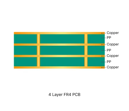
4 Layer FR4 PCB Production Record #FR4-20260113-031
| Parameter | Value | Parameter | Value |
|---|---|---|---|
| PCB Type | FR4 PCB | Quantity | 15 pcs |
| Layers | 4 Layers | Board Type | Panel PCB |
| Dimensions | 130 x 130 mm | Copper Weight | 1.5oz |
| Thickness | 1.2 mm | Min Track / Spacing | 6/6mil↑ |
| Surface Finish | ENIG (Immersion Gold) | Min Hole Size | 0.25mm |
| Solder Mask | Green | Silkscreen | White |
| Stack-up | Custom | Impedance Control | No |
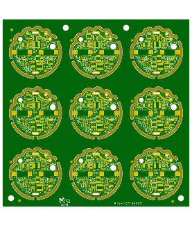
This 4-layer FR-4 order (130×130 mm, 1.2 mm finished thickness, Shengyi S1000-2M material) was produced in 3×3 panel format for a total of 135 pieces. Outer copper was 1.5 oz with 1 oz inner layers, minimum trace/space at 6 mil, 0.25 mm minimum hole size, and ENIG surface finish. V-cut combined with stamp holes supported customer-specified depanelization. Production was completed within the 11-day delivery window with 100% flying probe testing.
During CAM review, several DFM adjustments were required. Fiducial points on process edges received added protection rings to prevent detachment during handling, directly addressing risks observed in prior panelization and fiducial protection challenges. Stamp hole placement was optimized by removing the far-side holes to ensure clean separation without stressing individual 4-layer PCBs. Stackup was adjusted to our standard copper-clad cores while maintaining overall thickness and copper balance. UL marking requests were resolved by omission due to expired certification and limited space on small boards; solder mask openings followed standard pad clearance with silk screen confirmed off-pad.
All engineering clarifications were confirmed with the customer before release. Final boards met electrical and dimensional requirements with consistent ENIG coverage and clean edge quality after mechanical forming. The order shipped with electrical test reports and material certificates, demonstrating reliable execution for this standard-geometry multi-layer panelized run.
Standard multilayer solution offering practical routing density and controlled impedance for industrial and consumer electronics.

In-depth guide to the most frequent Engineering Queries (EQ) and DFM issues in Multilayer FR4 PCB (4/6/8+ layers) production. Real factory insights on stack-up confirmation, impedance control, copper balance, inner layer design, via treatment, registration, and practical prevention strategies.
| Order ID | PCB Type | Layers | Dimensions | Solder Mask | Surface Finish | Quantity | Action |
|---|---|---|---|---|---|---|---|
| FR4-20260520-046 | FR4 PCB | 2 | 94.21 x 275 | Green | ENIG (Immersion Gold) | 75 | View detail |
| FR4-20260519-001 | FR4 PCB | 10 | 67.6 x 42 | Green | Gold Plating | 20 | View detail |
| FR4-20260515-068 | FR4 PCB | 14 | 244 x 267 | Green | ENIG (Immersion Gold) | 10 | View detail |


