High-frequency 2-layer Rogers boards with thin 0.254mm profile and special surface requirements frequently present unique DFM challenges during CAM review. This case examines a 35.6 × 120.7 mm board using RO4350B material. During engineering analysis, several critical issues involving copper-to-edge clearance, vias on component pads, and material-specific processing were identified, requiring direct customer confirmation.
As a senior CAM engineer with extensive experience in RF and high-frequency fabrication, I always pay close attention to edge protection and via treatments on thin Rogers materials. In this order, the combination of tight edge clearances and vias placed directly under IC pads triggered multiple Engineering Questions (EQs) to protect signal integrity and assembly reliability.
Order Overview
This was a 2-layer high-frequency PCB ( #ROG-20260310-012 ) built on Rogers RO4350B material with >280 TG value, 0.254mm finished thickness, and 1oz copper on both layers. The design specified immersion silver surface finish, green solder mask on top only (no bottom solder mask), white silkscreen, 0.25mm minimum hole size, and 5mil line width/spacing. Production involved 100% flying probe testing, single-piece delivery, and mechanical forming. Quantity was 15 pieces.
The thin profile and high-frequency material made edge clearance, via filling, and material color considerations particularly important during DFM review.
Main Engineering Questions Found During CAM Review
1. Copper-to-Outline Edge Clearance Risks
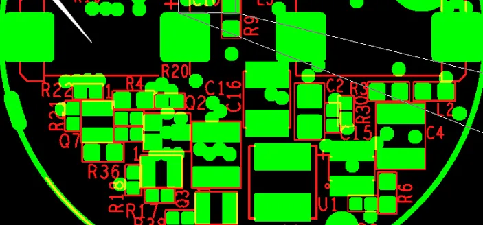
Multiple areas showed copper features positioned too close to the final board outline. We identified this during outline and copper layer review as a significant risk for exposed copper after routing or scoring.
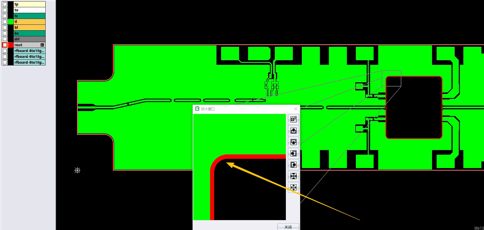
Figure 1: copper features positioned too close to the final board outline
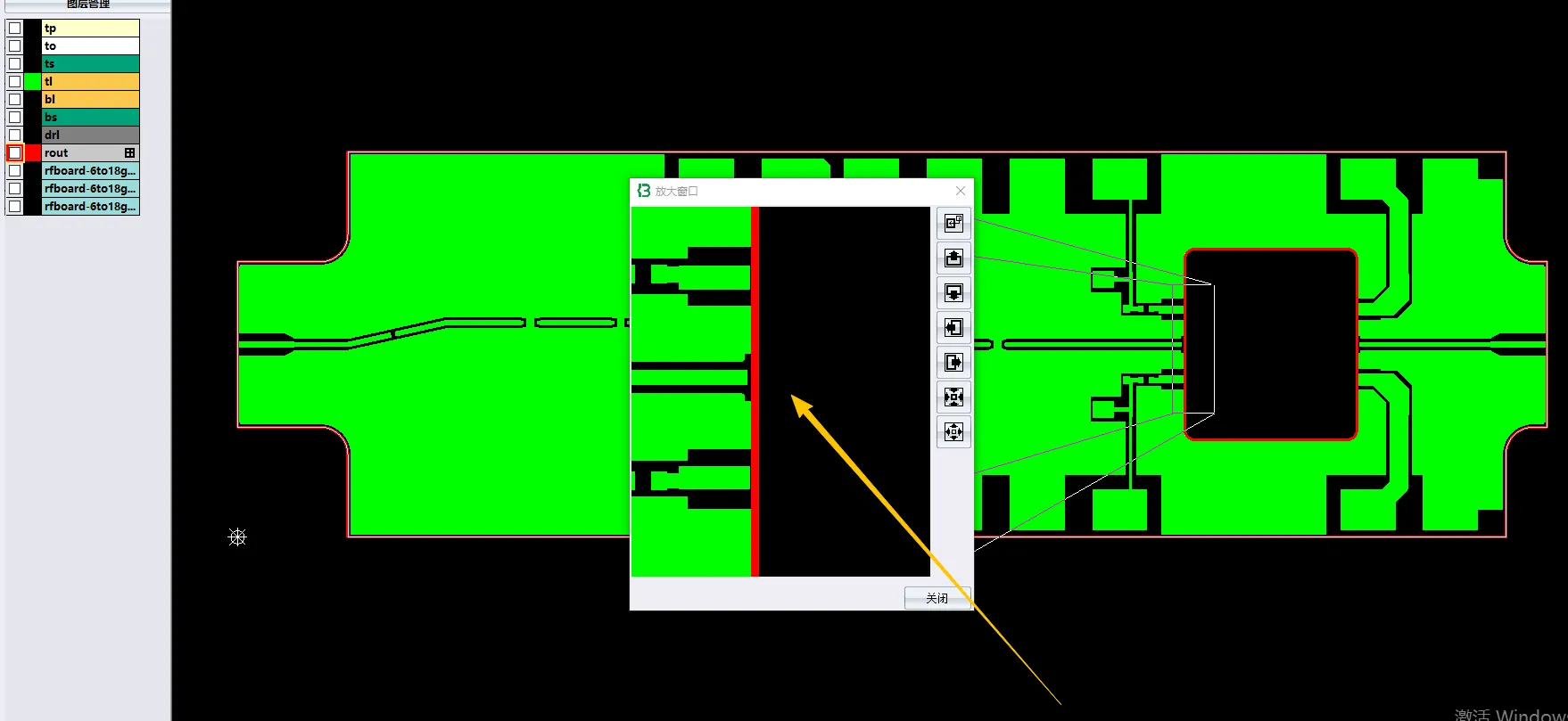
Figure 2: pads positioned too close to the final board outline
Our CAM engineer raised an EQ because on thin high-frequency materials like RO4350B, insufficient clearance can lead to copper peeling or shorting at the edges. We recommended increasing the clearance to provide a safe margin for mechanical forming and handling.
If this issue had been ignored, exposed copper at the board edges could cause short circuits during assembly or in the field, along with cosmetic defects and potential corrosion. Rogers materials are particularly sensitive to edge quality due to their high-frequency performance requirements. Based on IPC-2221 guidelines, adequate copper-to-edge spacing is essential for reliability.
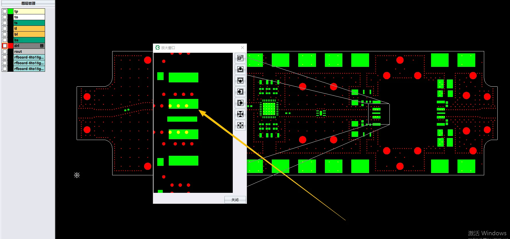
2. Vias Located on IC Pads - Resin Plug Recommendation
Several vias were designed directly under IC solder pads. We noticed this configuration during pad and via overlay analysis. Without resin plugging, these vias would create voids in the pads after soldering, leading to poor solder joint reliability.

Figure 3: vias located on IC pads
Our engineering team suggested using resin plugged vias for these locations. We asked the customer to confirm whether they accepted the risk of potential voids or preferred the additional plugging process. This is a common concern on high-density RF boards where via-in-pad is used for better signal performance.
If ignored, the vias could cause solder wicking, resulting in insufficient solder on pads, weak joints, tombstoning, or complete open circuits after reflow. Resin plugging helps maintain pad planarity and reliability in such designs.
3. Large Solder Mask Openings and Marking Placement
The customer requested additional marking on the board. However, we noticed that several solder mask openings were significantly larger than standard. Our CAM team identified that adding markings in these areas would place them directly on the exposed copper surface rather than on solder mask.
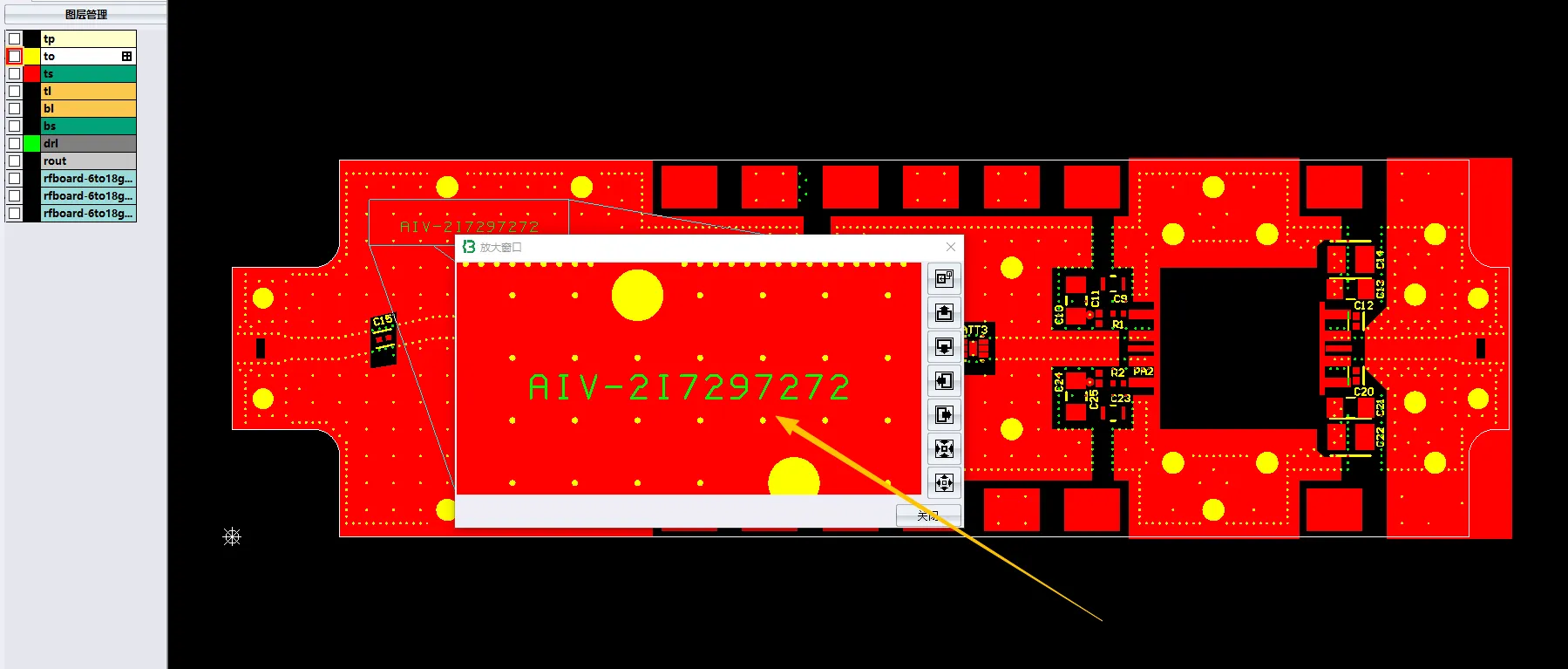
Figure 4: solder mask openings were significantly larger than standard
We raised an EQ to confirm whether this surface placement was acceptable, as markings on bare copper can have different adhesion and durability characteristics compared to standard silkscreen on mask. On high-frequency boards, large openings are sometimes intentional for performance, but they limit marking options.
If not clarified, markings could suffer from poor adhesion, smudging, or readability issues after assembly and handling. We recommended reviewing the marking content and location to ensure it would not interfere with RF performance or component areas. The customer confirmed the placement, allowing us to proceed with surface marking where necessary.
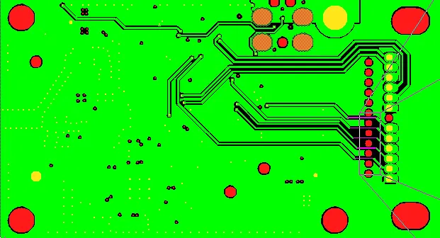
4. 2.1mm Holes Marked as Non-Plated but Containing Circuit Layers
Two 2.1mm holes were explicitly marked as non-metallized (NPTH) in the drill file. However, these holes overlapped with circuit layers, creating a potential conflict. We noticed this during drill-to-copper overlay review and raised an EQ for confirmation.
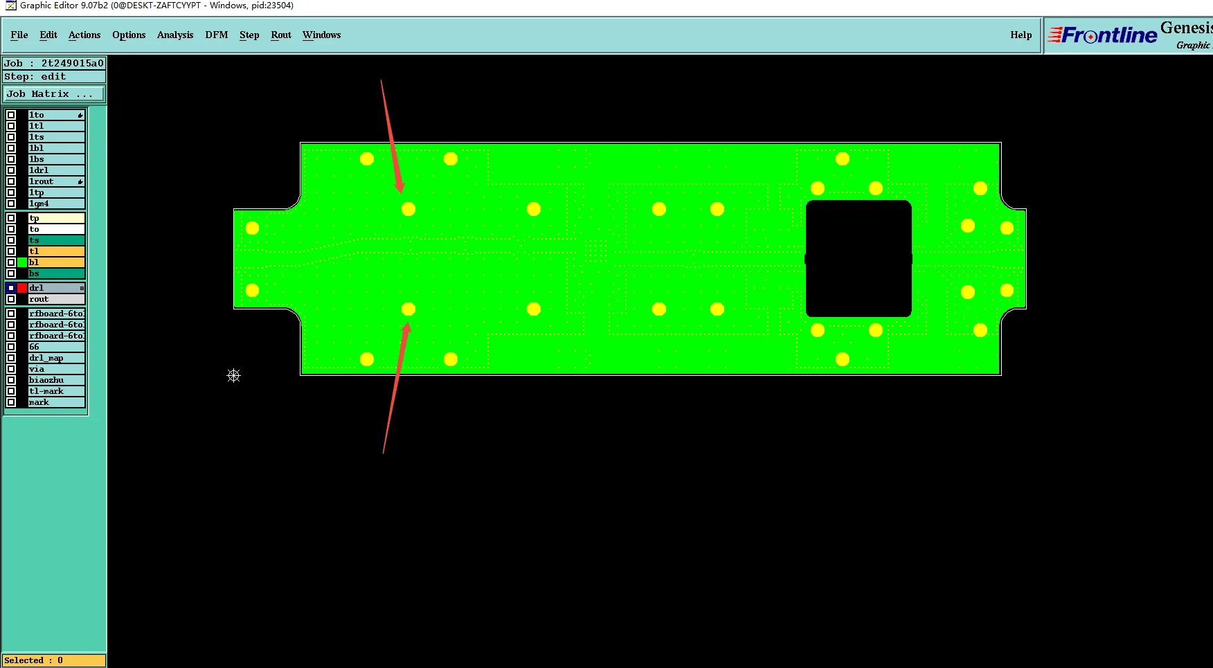
Figure 5: NPTH overlapped with circuit layers
Treating them as non-plated while having copper features nearby could lead to unintended copper exposure inside the hole or shorting risks. Our engineer asked whether these holes should remain non-plated or be processed as plated through holes with appropriate clearance.
Without confirmation, this mismatch could result in open circuits, exposed copper inside the holes, or drilling/plating defects. The customer clarified the intent, and we adjusted the production data to maintain consistency between drill definitions and copper features.
5. No Bottom Solder Mask on Rogers Material and Slot Size Inconsistencies
The design specified no bottom solder mask on this Rogers RO4350B board. During our mask layer review, we identified that omitting the bottom solder mask on high-frequency materials like Rogers often results in visible yellowing of the base material after processing. We raised an EQ to confirm whether the customer accepted this aesthetic change, as it is a common trade-off for maintaining optimal RF performance.
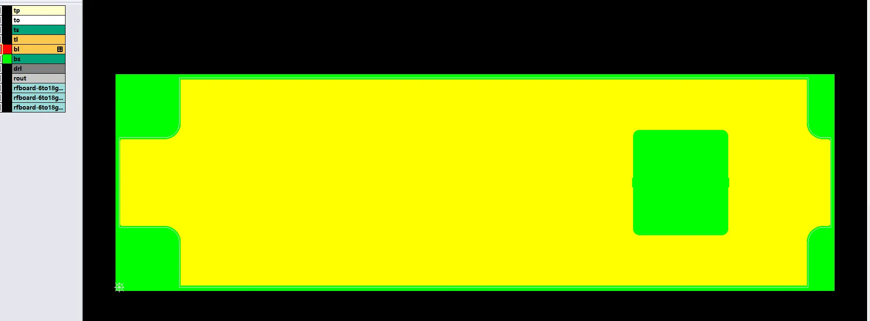
Figure 6: no bottom solder mask on this Rogers RO4350B board
Additionally, slot sizes between the GM and GM4 layers showed inconsistencies in dimensions. We noticed this discrepancy while comparing the mechanical and outline layers. Our CAM engineer asked for confirmation on which layer represented the authoritative slot size to avoid dimensional errors during routing and scoring.
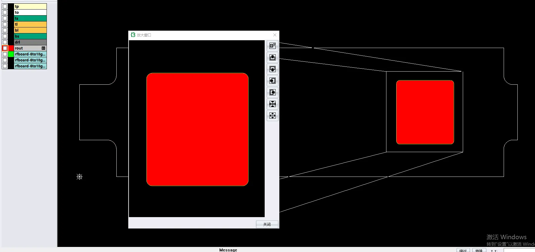
Figure 7: slot size inconsistencies between the GM and GM4 layers
We have seen cases where unconfirmed no-bottom-mask decisions lead to customer surprise regarding board appearance, while inconsistent slots can cause misalignment in final mechanical features or assembly problems. On thin high-frequency boards, such issues can affect both cosmetic acceptance and functional performance. If left unresolved, the board might fail customer visual inspection or have incorrect cutouts, leading to scrap or rework.
After receiving explicit confirmation that the yellowing was acceptable and clarifying the correct slot dimensions, we updated the production files accordingly. This ensured the final boards met both electrical and mechanical expectations for this RF application.
Suggested EQ Categories
Hole & Tolerance Issues
- Copper-to-outline edge clearance
- Via-in-pad configuration and resin plugging
Material & Process Clarification
- No bottom solder mask on Rogers material (yellowing acceptance)
- Slot size inconsistency between layers
Manufacturing Risks and DFM Insights
On high-frequency thin boards, edge clearance is frequently overlooked. Insufficient spacing leads to exposed copper and reliability issues. Via-in-pad without plugging is another common pitfall that affects SMT yield on Rogers materials.
Ignoring the clearance EQ could result in edge shorts or delamination. Unplugged vias on pads risk solder defects and assembly failures. These problems typically cause delays, increased costs, and multiple review cycles.
How the Engineering Team Resolved the Issues
Our team provided magnified images showing the tight edge clearances and recommended adjustments. For the via-in-pad locations, we confirmed the need for resin plugging. The customer accepted the no-bottom-mask condition after understanding the potential yellowing of Rogers material. Slot sizes were reconciled with the authoritative layer.
We noticed the edge issues early and adjusted the production files after confirmation. This ensured high first-pass yield for this RF application.
Final Manufacturing Outcome
All EQs were resolved with customer approval. Edge clearances were optimized, via plugging confirmed where needed, and material expectations aligned. The order was released for production with updated manufacturing parameters.
Key Takeaways for PCB Designers
- Maintain adequate copper-to-outline clearance on high-frequency boards to prevent edge exposure and shorts.
- Consider resin plugging for vias placed directly under component pads to ensure reliable soldering.
- Explicitly confirm acceptance of material-specific characteristics, such as Rogers board yellowing without bottom solder mask.
- Ensure consistent slot and mechanical features across all relevant layers in Gerber data.
- Account for high-frequency material processing limitations when designing thin boards.
- Provide clear notes for any special via treatments or surface finish requirements.
- Review edge and via features thoroughly before submission for quotation.
- Be responsive to DFM suggestions regarding clearance and plugging to reduce risks.
FAQ
Q1: Why is copper-to-edge clearance critical on Rogers boards?
A1: Insufficient clearance leads to exposed copper after routing, causing shorts, corrosion, or signal degradation in high-frequency applications.
Q2: Should vias on IC pads always use resin plugging?
A2: Yes, especially on thin boards. Without plugging, vias create voids in pads, leading to weak solder joints and reliability risks.
Q3: What causes yellowing on Rogers material without bottom solder mask?
A3: Exposure of the base material during processing. Many customers accept this for performance reasons, but it should be explicitly confirmed.
Q4: Why confirm slot sizes across layers?
A4: Inconsistent slots can lead to mechanical misalignment or incorrect final dimensions after routing.