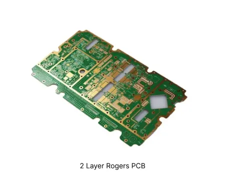
PCB Specifications
| Parameter | Value | Parameter | Value |
|---|---|---|---|
| PCB Type | Rogers PCB | Quantity | 15 pcs |
| Layers | 2 Layers | Board Type | Single PCB |
| Dimensions | 35.6 x 120.7 mm | Copper Weight | 1oz |
| Thickness | 0.254 mm | Min Track / Spacing | 5/5mil |
| Surface Finish | Immersion Silver | Min Hole Size | 0.25mm |
| Solder Mask | Green | Silkscreen | White |
| Material Type | Rogers/RO4350B |
Manufacturing Timeline
Logistics Information
Key Manufacturing Processes
Manufacturing Summary
This 2-layer high-frequency board measured 35.6 × 120.7 mm with 1 oz copper on both sides and a thin 0.254 mm finished thickness using Rogers RO4350B material. Produced as single pieces in a quantity of 15, the design featured 5 mil line/space, immersion silver surface finish, and no process edges. No blind vias were present, with mechanical forming and 100% flying probe testing. The combination of Rogers substrate, tight geometry, and edge proximity presented the main production considerations.
DFM review confirmed multiple file details including inconsistent slot dimensions between layers and non-plated hole designations where circuit features existed. Copper features and pads positioned very close to the board outline risked edge exposure during routing. Vias located directly on IC pads raised concerns for potential voids and solder joint reliability, prompting discussion of resin plugging. The absence of bottom solder mask on Rogers material was noted for possible yellowing. Edge clearance adjustments and file confirmations were implemented to balance design intent with manufacturability. Rogers material edge clearance handling was applied to minimize copper exposure while preserving electrical performance.
Production completed successfully within 14 days, delivering boards that met dimensional, electrical, and surface finish requirements. The thin high-frequency panels maintained stability throughout processing and testing, supporting reliable RF performance for this order.
Explore More PCB Manufacturing Resources
2 Layer Rogers PCB Manufacturing Insights
Rogers high frequency laminates demand specialized processing to maintain dielectric stability and signal integrity in RF designs.
Troubleshooting Common Manufacturing Challenges with Rogers PCBs
Master troubleshooting common Rogers PCB manufacturing challenges including drilling defects, plating adhesion, delamination, and CTE mismatch. Learn practical solutions, process adjustments, and DFM tips to improve yield for high-frequency RO4000, RO4350B, and PTFE-based boards.
Real Production Records
| Order ID | PCB Type | Layers | Dimensions | Solder Mask | Surface Finish | Quantity | Action |
|---|---|---|---|---|---|---|---|


