Introduction
High-density interconnect (HDI) PCBs represent a cornerstone of advanced PCB technology, enabling compact designs with superior routing density through features like microvias and blind or buried vias. As electronic devices demand smaller form factors and higher performance, engineers face significant challenges in ensuring reliability under thermal, mechanical, and electrical stresses. IPC-6012 serves as the primary qualification and performance specification for rigid printed boards, including those with HDI structures. This standard outlines rigorous criteria to validate board integrity, from material selection to final assembly readiness. By adhering to IPC-6012, designers and manufacturers mitigate risks associated with microvia failures and warpage in complex stackups. This article explores how IPC-6012 addresses these advanced design challenges in HDI PCB fabrication.
What Is IPC-6012 and Why It Matters for HDI PCBs
IPC-6012 defines qualification and performance requirements for rigid printed boards, encompassing single-sided, double-sided, and multilayer constructions with plated-through holes, blind vias, buried vias, and microvias typical in HDI PCBs. It establishes performance classes, primarily Class 2 for dedicated service and Class 3 for high-reliability applications, that dictate stricter tolerances as complexity increases. For HDI PCBs, which integrate high-density interconnect features to support fine-pitch components, the standard ensures boards withstand operational stresses without degradation. Compliance verifies electrical continuity, mechanical stability, and environmental durability, critical for applications in telecommunications, computing, and aerospace. Without these guidelines, advanced PCB technology risks field failures due to via cracking or delamination in stacked microvia configurations. Engineers rely on IPC-6012 to bridge PCB design intent with manufacturable outcomes.
IPC-6012F Updates and HDI-Specific Addendums
The 2023 IPC-6012F revision introduced several changes directly benefiting HDI manufacturing. One of the most significant is the reduction of the default minimum dielectric thickness to 65 μm (2.56 mil) for new designs released after December 31, 2023. This adjustment accommodates the thin dielectrics (typically 60–100 μm) required for laser-drilled microvias while preventing unnecessary non-conformance issues during fabrication.
Additional F-revision highlights include:
- Updated test coupon designs specifically for evaluating stacked and staggered microvia reliability under thermal cycling and interconnect stress testing (IST).
- Revised allowances for initial copper foil reduction (up to 50% in certain cases after processing).
- Strengthened language on copper wrap plating and void acceptance criteria for high-aspect-ratio microvias.
- Enhanced focus on CAF resistance and electromigration in dense HDI layouts.
The IPC-6012DS addendum applies to defense, space, and other mission-critical applications. It imposes stricter controls on material traceability, manufacturing environment, testing frequency, and documentation compared to the base IPC-6012 standard. For HDI boards, IPC-6012DS often requires additional microsection sampling, tighter bow-and-twist limits, and validated stacked microvia performance beyond two levels.
These updates reflect industry experience showing that two-level stacked microvias are generally reliable with proper materials, while three-or-more-level stacks demand rigorous qualification. IPC-6012F and its addendums help manufacturers reduce qualification time while improving long-term reliability in advanced HDI designs.
Key Technical Principles in IPC-6012 for HDI Structures
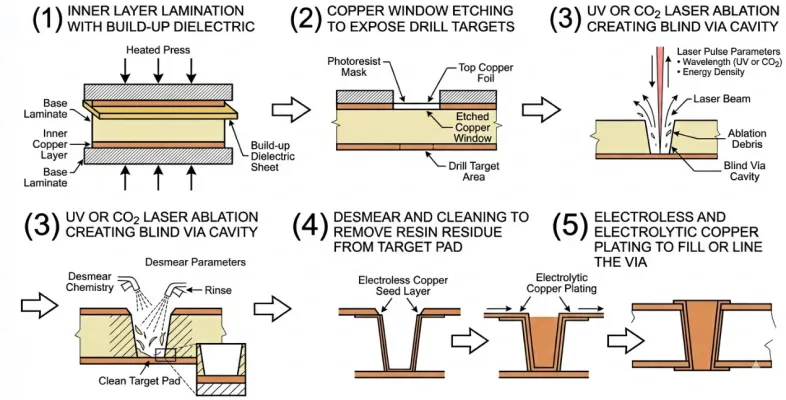
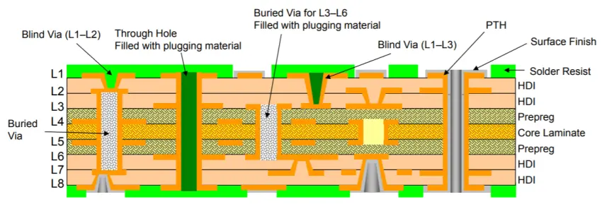
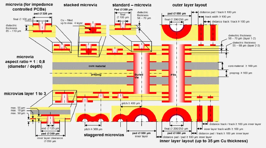
HDI PCBs leverage microvias, laser-drilled interconnects with high aspect ratios, to achieve routing densities unattainable with conventional vias, but this introduces reliability concerns like plating voids and thermal expansion mismatches. IPC-6012 addresses these by specifying microsection evaluation criteria for via integrity, including copper thickness, etchback, and smear removal in drilled holes. Recent revisions emphasize reliability testing for interconnected via structures, such as stacked and staggered microvias, through dedicated test coupons that simulate real-world stresses. The standard also covers internal plated layers, allowing optimized thicknesses for thinner dielectrics common in HDI stackups while maintaining signal integrity. Conductor spacing and annular ring requirements prevent shorts and breakouts, particularly stringent in Class 3 where external layer tolerances prohibit certain imperfections. These principles ensure HDI PCBs maintain performance across lamination cycles and sequential build-up processes. For detailed implementation strategies, see our companion guide to sequential lamination in HDI PCBs.
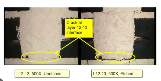
Bow and twist limitations in IPC-6012 counteract warpage induced by asymmetric copper distribution or thin core materials in high-layer-count HDI boards. Warpage compromises via registration and component mounting, leading to assembly defects. The standard mandates dimensional stability checks post-lamination and after thermal conditioning, validating flatness under heat. Copper wrap plating requirements enhance via barrel strength, reducing risks of cracking during reflow or cycling. Dimples and protrusions in filled microvias receive defined acceptance levels, balancing fabrication yields with long-term reliability. Overall, these mechanisms support advanced PCB technology by quantifying tolerances for high-density interconnect features.
Table: Key IPC-6012 Requirements for HDI Microvias (Class 2 vs Class 3)
| Parameter | Class 2 Typical | Class 3 Typical | HDI Impact |
|---|---|---|---|
| External Annular Ring | 1–2 mil (breakout allowed in some cases) | 2 mil minimum, no breakout | Prevents pad lifting in fine-pitch components |
| Copper Wrap/Plating (Microvias) | 12 μm average | 20 μm average, 6 μm wrap min | Critical for stacked via thermal cycling reliability |
| Filled Via Protrusion | ≤75 μm | ≤50 μm (1.96 mil) | Affects solder joint planarity |
| Bow & Twist (Thin Boards) | ≤1.0–1.5% | ≤0.75% | Maintains registration in multilayer HDI |
| Minimum Dielectric (Post F) | 65 μm (new default) | 65 μm (new default) | Enables higher density laser microvias |
Advanced Design Challenges and IPC-6012 Solutions
Microvia reliability stands as a primary challenge in HDI PCB design, where stacked configurations amplify electromigration and CAF failures under high currents and temperatures. IPC-6012 introduces performance-based testing, including interconnect stress tests and thermal shock simulations, to qualify these structures without opens or increased resistance. Engineers must consider dielectric spacing minima to avoid breakdowns in dense routing, with the standard providing updated criteria aligned with finer geometries. Plating uniformity across blind vias and microvias prevents voids at interfaces, addressed through microsection analysis and acceptance rules for internal layers. For back-drilled structures in HDI boards, clarified depth measurements exclude surface artifacts, ensuring stub removal without damaging adjacent conductors. Engineers should also review material selection criteria for high-performance HDI boards when balancing CTE and dielectric performance.
Another hurdle involves cavities and edge plating in complex HDI layouts, where metallization continuity supports embedded components or shielding. IPC-6012 defines cavity types and plating void allowances, specifying tolerances for depth and wall coverage to maintain structural integrity. Solderability preservation after multiple lamination cycles requires controlled surface finishes and dewetting criteria, preventing assembly issues. Printed board cavities demand conductor setbacks from edges to avoid bridging during plating. These solutions enable engineers to push HDI limits while qualifying boards for Class 3 environments.
Table: Class 2 vs Class 3 Decision Matrix for HDI PCBs
| Application Type | Reliability Requirement | Recommended Class | Key IPC-6012 Differences | When to Choose |
|---|---|---|---|---|
| Consumer electronics, prototypes | Moderate | Class 2 | Allows some breakout, lower plating thickness, reduced testing frequency | Cost-sensitive, non-mission-critical |
| Telecom infrastructure, automotive | High | Class 3 | No external breakout, 2 mil external annular ring, higher copper wrap, increased microsection sampling | Thermal cycling, long service life |
| Aerospace, medical implants | Mission-critical | Class 3 + DS addendum | Stricter documentation, enhanced IST/thermal shock, tighter bow/twist | Failure cannot be tolerated |
Class 3 demands tighter tolerances, more frequent qualification testing, and higher minimum copper thickness, making it essential for HDI boards in harsh environments. The decision should be made early in the design phase and clearly called out on fabrication drawings.
Best Practices for IPC-6012 Compliance in HDI PCB Design
Start with symmetric stackups to minimize warpage, balancing copper weight across layers and selecting low-CTE materials compatible with microvia drilling. Specify Class 3 early for high-reliability HDI PCBs, as it enforces tighter annular rings and prohibits breakout on external pads, demanding precise layer-to-layer registration. Incorporate IPC-6012 test coupons in panel designs to verify microvia performance post-thermal stress, focusing on stacked vias prone to failure. Optimize via-in-pad configurations with conductive fills to enhance thermal dissipation in high-density interconnect areas. Conduct 100% electrical testing and sample microsections per lot, escalating to full lot verification for critical features. These practices align with our broader HDI PCB design guide for overcoming density challenges.
Leverage IPC-A-600 for visual acceptance alongside IPC-6012 performance metrics, ensuring solder mask adhesion and hole cleanliness meet HDI tolerances. Document starting versus finished copper thicknesses to avoid etching losses in internal layers. Simulate reflow profiles during design to preempt delamination risks in sequential build-ups. Collaborate with fabricators on aspect ratios and lamination parameters tailored to microvia reliability. These practices streamline qualification, reducing iterations in advanced PCB technology development.
Troubleshooting Common HDI Issues Under IPC-6012
Engineers often encounter via dimpling in filled microvias, where excess resin protrudes post-cure; IPC-6012 limits these to functional levels on soldered lands, rejecting only if they compromise assembly. Plating separations in edge-plated HDI grounds signal poor adhesion—inspect for anchor extensions and wrap plating per standard tables. Warpage exceeding bow and twist maxima post-bake indicates core instability; remedy with constrained lamination or active metal cores. Thermal stress failures like barrel cracks trace to inadequate etchback; verify smear removal via cross-sections. Dewetting on surfaces post-multiple reflows violates solderability—select ENIG or compatible finishes as defaults.
Stacked microvia opens under cycling stem from CTE mismatches; IPC-6012's updated coupons isolate these, guiding material swaps to resin-coated copper. Internal plane voids require dielectric flow control during pressing. Address drill wander in blind vias with stepped drilling sequences. Routine AOI catches early misregistration, while X-ray confirms fill in staggered structures. Systematic adherence resolves these, upholding HDI PCB reliability.
Building an IPC-6012 Compliant HDI Workflow
A robust workflow integrates early fabricator collaboration, comprehensive DFM reviews, and iterative qualification. Share complete stackup drawings, material specifications, and reliability requirements before tape-out. Request capability reports confirming their ability to meet IPC-6012F microvia plating and warpage limits.
Recommended DFM Checklist:
- Validate all microvia aspect ratios against fabricator capabilities.
- Confirm symmetric copper distribution and balanced construction.
- Specify via fill type, cap plating thickness, and protrusion limits.
- Include multiple test coupons per panel for IST and microsection.
- Define acceptance criteria for bow/twist, annular rings, and dielectric thickness.
- Require full traceability and process control data for Class 3/DS boards.
- Plan for future geometries — discuss capability roadmaps for smaller microvias and higher layer counts.
Future trends point toward even smaller microvias (aspect ratios approaching 1:1), hybrid stacked/staggered designs, and tighter integration with embedded components. Staying aligned with evolving IPC-6012 revisions will remain essential for maintaining HDI PCB compliance at the cutting edge.
Conclusion
IPC-6012 equips engineers with a robust framework to tackle HDI PCB challenges, from microvia reliability to warpage control in high-density interconnect designs. Its performance classes and testing protocols ensure advanced PCB technology meets demanding applications without compromise. By integrating these guidelines into PCB design workflows, teams achieve qualification efficiency and field durability. Future revisions will likely refine stacked via criteria amid shrinking geometries. Prioritizing IPC-6012 compliance elevates HDI fabrication from art to engineered precision.
FAQs
Q1: What role does IPC-6012 play in qualifying microvias for HDI PCBs?
A1: IPC-6012 establishes performance tests for microvias in high-density interconnect boards, including thermal stress and microsection evaluations to detect plating defects or cracks. It defines acceptance for dimples, protrusions, and voids in stacked structures, ensuring reliability under operational loads. Class 3 requirements heighten scrutiny for advanced PCB technology, mandating coupon-based validation. This prevents failures in compact designs with fine-pitch routing.
Q2: How does IPC-6012 address warpage in HDI PCB design?
A2: The standard specifies bow and twist limits post-lamination and thermal conditioning, critical for multilayer HDI PCBs prone to distortion from thin dielectrics. Symmetric stackups and material selection align with these to maintain via registration. Qualification after reflow simulation confirms dimensional stability. Engineers use this to optimize high-density interconnect layouts for assembly success.
Q3: Why choose Class 3 under IPC-6012 for advanced HDI applications?
A3: Class 3 demands stricter plating thickness, annular ring integrity, and no external breakouts, ideal for high-reliability HDI PCBs in mission-critical systems. It includes enhanced testing frequency for microvias and internal layers. This elevates PCB design quality, reducing risks in thermal cycling. Compliance supports cutting-edge advanced PCB technology deployments.
Q4: What testing ensures IPC-6012 HDI PCB compliance?
A4: Key tests cover electrical continuity, thermal shock via solder float, and interconnect stress for microvias in high-density interconnect boards. Microsections verify copper wrap and dielectric spacing. Visual and dimensional inspections per IPC-A-600 complement performance checks. These validate rigid board robustness across fabrication stresses.
References
IPC-6012F — Qualification and Performance Specification for Rigid Printed Boards. IPC, 2023
IPC-A-600K — Acceptability of Printed Boards. IPC, 2020
IPC-2226B — Sectional Design Standard for High Density Interconnect (HDI) Printed Boards. IPC, 2018