Introduction to Capacitive Touch Sensing
Touchscreens have become the dominant user interface in consumer electronics, industrial equipment, automotive systems, medical devices, and commercial kiosks due to their intuitive operation. Among various technologies, projected capacitive touch using charge-transfer methods-particularly in transverse (mutual capacitance) mode-offers superior performance in accuracy, multi-touch support, durability, and optical clarity compared to older resistive designs.
Earlier Touch Technologies and Limitations of Resistive Panels
Early touch solutions included infrared beam interruption and surface acoustic wave systems. While functional, they were costly and unsuitable for mass-market adoption.
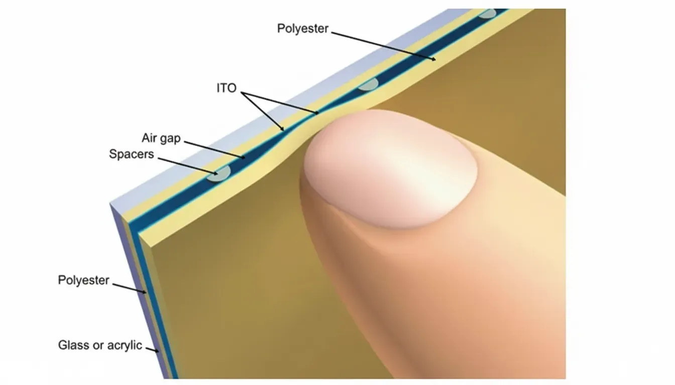
Resistive touch panels, dominant since the 1970s, use two transparent conductive layers (typically ITO on glass and flexible PET) separated by spacer dots. Pressure from a finger or stylus creates contact, forming a voltage divider whose output is measured to determine X/Y coordinates. Variants include 4-wire, 5-wire, 6-wire, and 8-wire configurations for different sizes and resolutions.
Advantages of resistive technology include simple interfacing (voltage gradients read via ADCs) and low cost. However, significant drawbacks limit its use in modern applications:
- Multilayer stack reduces optical transmission (often ~75%) and introduces haze.
- Susceptible to scratches, wear, and alignment issues.
- Poor multi-touch support.
- Sensitive to electrical noise (e.g., from underlying LCDs), requiring filtering that slows response.
- Lower accuracy and durability under heavy use.
These limitations drove the industry shift toward capacitive sensing.
Charge-Transfer Techniques in Capacitive Sensing
Capacitive controllers employ several methods: RC time-constant measurement, AC current sensing, and charge-transfer. Charge-transfer approaches stand out for their robustness.
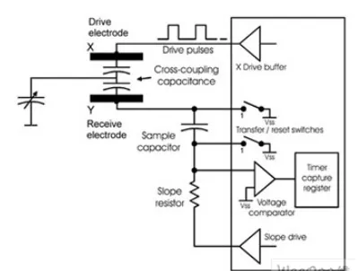
Single-Ended Charge-Transfer: Uses one electrode per channel. CMOS switches transfer charge from the sense capacitor (Cx, modulated by finger proximity) to a larger sampling capacitor (Cs). The number of charge-transfer cycles needed to reach a threshold voltage is measured. This method offers good noise immunity due to low impedance and large Cs.
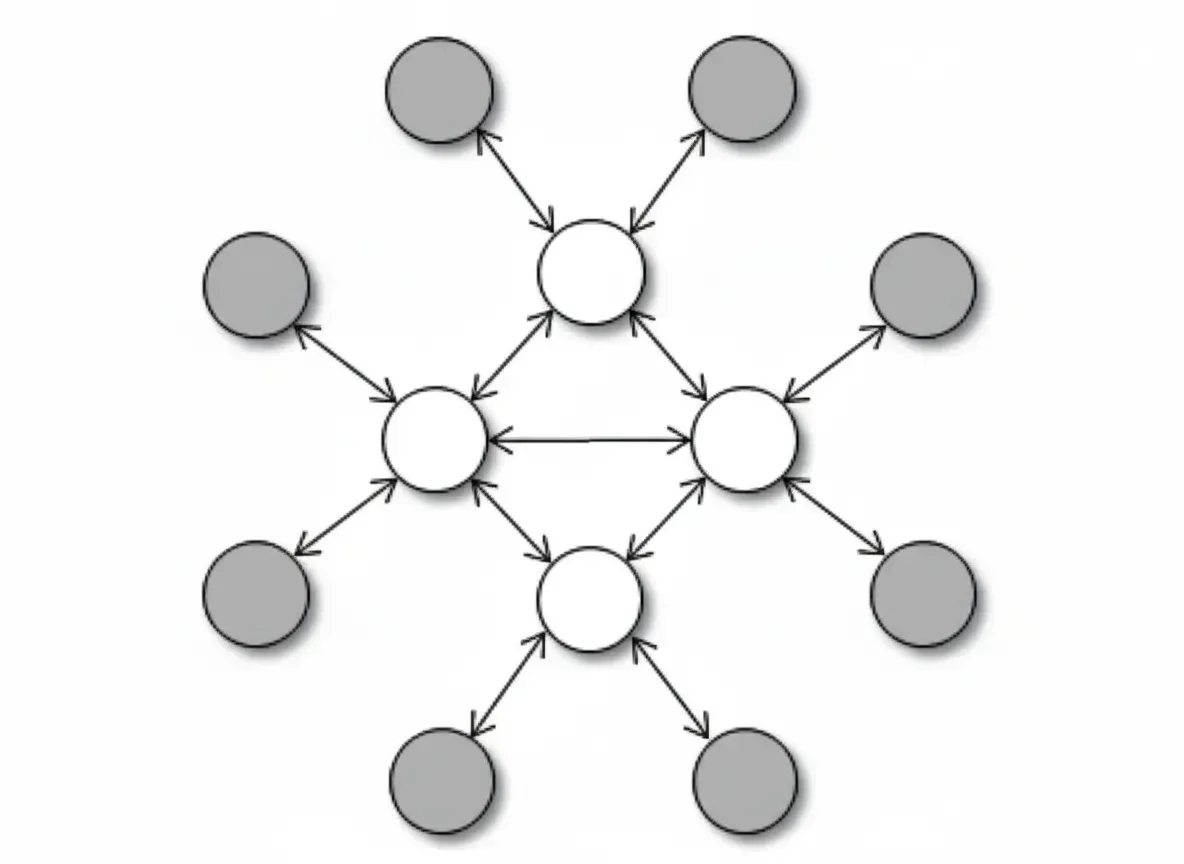
Transverse-Mode (Mutual Capacitance) Charge-Transfer Sensing
Transverse-mode (or mutual capacitance) sensing uses a matrix of transmit (drive) and receive electrodes. A drive pulse on one axis couples charge to the receive axis; a finger touch alters this coupling by shunting charge to ground.
Key Advantages:
- Excellent multi-touch detection and ghosting rejection.
- Self-shielding properties improve noise immunity.
- Reduced routing complexity and faster scanning (simultaneous measurement along drive lines).
- Lower power consumption.
- Support for operation through thick overlays (glass, plastic) and better environmental robustness.
The technique resembles a T-bridge network where finger capacitance (Cx) attenuates the transmitted signal. Advanced implementations combine spread-spectrum modulation, DSP, and dual-slope conversion for stability against LCD noise, moisture, and temperature variations.
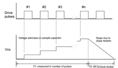
Pulse-Train Sampling and Zero-Cross Timing
Controllers apply pulse trains to drive electrodes, accumulating charge on sampling capacitors. After the train, a controlled discharge ramp is generated, and the time to zero-crossing (detected by a comparator) is measured. This time is proportional to the coupling capacitance and decreases with touch.
Benefits of this approach:
- Automatic compensation for supply variations and component tolerances.
- Inherent moisture suppression (short gate times minimize water film effects modeled as distributed RC).
- Strong RF and EMI immunity.
- Adjustable pulse count for optimizing gain across different panel thicknesses and materials.
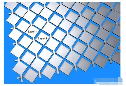
Single-Layer and Multi-Touch Designs
Traditional projected capacitive screens use multiple ITO layers, reducing transparency. Transverse-mode controllers support single-layer electrode patterns (e.g., proprietary diamond or interdigitated designs), offering:
- Higher light transmission.
- Thinner, lighter, and lower-cost construction.
- Simplified lamination.
For advanced dual-axis multi-touch, dual-layer or optimized single-layer matrices enable simultaneous detection of multiple fingers with distinct field signatures, supporting gestures and precision input.
Relevance to PCB Design and Manufacturing
Capacitive touch implementations place significant demands on supporting PCBs:
- Electrode Integration: Flexible or rigid PCBs can incorporate transparent conductive patterns or connect to ITO films on glass/plastic.
- Controller Integration: Low-noise power supplies, decoupling, and short traces between electrodes and controller ICs minimize parasitics.
- Signal Integrity: Controlled impedance, shielding layers, and careful grounding reduce noise coupling from displays or other electronics.
- HDI and Flex Circuits: Enable compact integration in wearables, automotive dashboards, or industrial panels.
- Manufacturing Precision: Tight tolerances on trace widths/spacing, impedance control, and surface finishes ensure consistent sensitivity and multi-touch accuracy across production volumes.
Expert PCB assembly supports reliable bonding of flex tails, component placement for ESD protection, and overall system reliability.
Conclusion
Transverse-mode charge-transfer capacitive touch delivers a robust, high-performance solution that overcomes resistive limitations while enabling thinner, clearer, and more capable interfaces. Its noise immunity, multi-touch support, and compatibility with single-layer designs make it ideal for modern electronics. Continued advances in controller ICs and PCB integration will further expand its adoption.
FAQ
Q1: How does transverse-mode differ from single-ended capacitive sensing?
A1: Transverse-mode uses mutual capacitance between drive and sense electrodes for better multi-touch performance and noise rejection compared to self-capacitance (single-ended) methods.
Q2: What are the main advantages over resistive touch?
A2: Superior optical clarity, durability, multi-touch capability, faster response, and better environmental robustness.
Q3: Why is PCB design important for capacitive touch performance?
A3: It affects noise levels, signal integrity, power quality, and mechanical integration of the electrode matrix and controller.