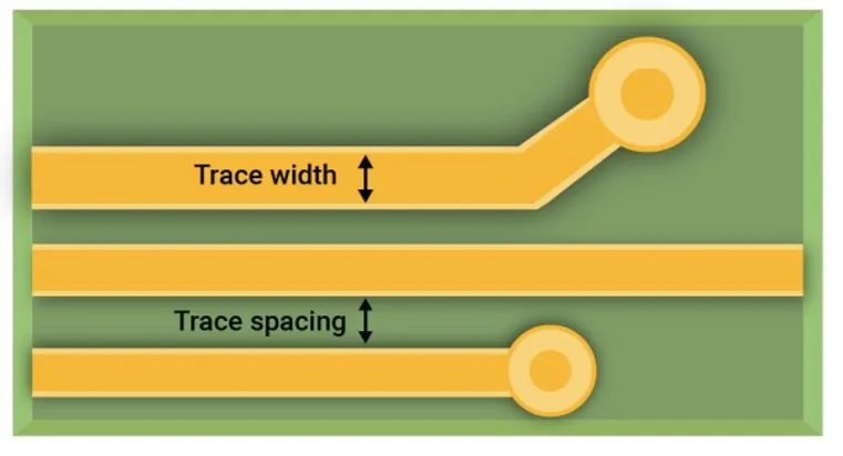
Trace Width
Trace width is a fundamental aspect of printed circuit board (PCB) design that directly influences the performance, reliability, and safety of electronic circuits. In PCB layouts, trace width refers to the dimension of the copper conductors that carry electrical signals and power between components. Selecting the appropriate trace width is essential to handle current loads without excessive voltage drop, overheating, or signal degradation, which can lead to failures in applications ranging from consumer electronics to industrial systems. For engineers and hobbyists searching for information on trace width, this tag serves as a comprehensive resource to address common challenges in circuit design. Key considerations include calculating trace width based on factors such as current rating, ambient temperature, and copper thickness, often guided by standards like IPC-2152. Practical tools like online trace width calculators can simplify this process, allowing users to input parameters and receive precise recommendations. For instance, wider traces are crucial for high-current paths to minimize resistance and heat buildup, while narrower traces suit high-density boards where space is limited, provided they maintain signal integrity. Best practices emphasize starting with conservative estimates and verifying through simulations or prototypes to avoid issues like thermal hotspots or electromagnetic interference. This tag gathers articles that delve into these topics, offering step-by-step tutorials on trace width optimization for various scenarios, including multilayer PCBs and RF designs. By reviewing the content here, designers can gain insights into adapting trace widths for specific projects, ensuring robust and efficient electronic assemblies that meet regulatory requirements and perform reliably over time.
Technical Articles
Maximizing Efficiency: Effective Strategies for PCB Routing
The Ultimate Copper Thickness (Mils) Conversion Chart for PCB Design
Optimize Your CEM 1 PCB Design: Mastering Trace Width and Spacing

Design Considerations for IPC Class 2 PCB Assembly: A Comprehensive Guide
Spacing Secrets: Mastering Trace Width for High Voltage PCBs
The Impact of PCB Trace Width on Solar Inverter Efficiency: A Detailed Analysis
Get in Touch
Send Message
- Products & Service
- Company
- About AIVON
- Contact
- News
- Blog
- Certification
-


- Payment
-


2026 AIVON.COM All Rights Reserved