Introduction
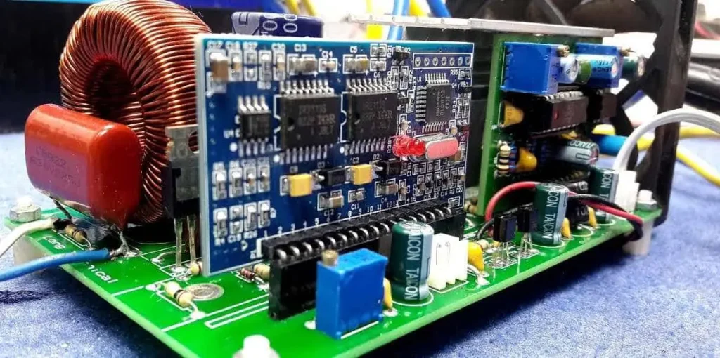
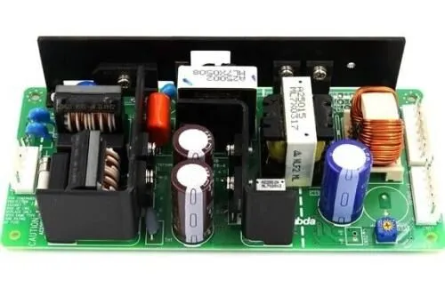
Solar inverters play a crucial role in photovoltaic systems by converting direct current from solar panels into alternating current for grid integration or local use. Efficiency in these devices directly influences overall system performance, energy yield, and operational costs. PCB trace width emerges as a critical design parameter in solar inverters, where high currents flow through power paths. Narrow traces can lead to excessive resistance, heating, and power dissipation, undermining solar inverter efficiency. Conversely, optimized trace widths enhance current carrying capacity while minimizing losses. This analysis explores how PCB trace width impacts key aspects like power loss and impedance, providing engineers with actionable insights grounded in established principles.
Understanding PCB Trace Width and Its Relevance to Solar Inverters
PCB trace width refers to the lateral dimension of conductive paths etched onto the board, typically measured in mils or millimeters. This dimension fundamentally determines the cross-sectional area available for current flow, alongside copper thickness. In solar inverters, which handle substantial DC and AC currents from panel arrays, inadequate trace width results in voltage drops and thermal buildup. Engineers must balance trace width with board space constraints, layer count, and routing density to maintain high solar inverter efficiency. Industry standards like IPC-2221 provide foundational guidelines for selecting trace widths based on expected loads and environmental factors. Proper sizing ensures reliable operation under varying solar irradiance and load conditions.
Wider traces reduce resistance per unit length, allowing higher current carrying capacity without exceeding allowable temperature rises. Solar inverters often operate in enclosed environments with limited airflow, amplifying the need for conservative designs. Trace width also influences electromagnetic compatibility by affecting loop areas and inductance. For power stages involving IGBTs or MOSFETs, trace width optimization prevents hotspots that could degrade components over time. This parameter thus bridges electrical performance and thermal management in demanding applications.
Technical Principles: Current Carrying Capacity and Its Effect on Efficiency
Current carrying capacity defines the maximum steady-state current a trace can handle while keeping temperature rise within limits, typically 10 to 20 degrees Celsius above ambient. According to IPC-2152, this capacity depends on trace width, copper weight, board thickness, and proximity to other conductors or planes. Narrow traces exhibit higher resistance, leading to I squared R losses that convert electrical energy into heat, directly reducing solar inverter efficiency. In high-power paths, such as DC bus links, insufficient width causes electromigration and voiding over cycles. Engineers calculate capacity using empirical charts or simulation tools aligned with these standards to predict performance.
Heat dissipation from traces occurs via conduction to adjacent layers, convection to air, and radiation, all enhanced by greater surface area from wider traces. External factors like board population density and airflow further modulate capacity. In solar inverters, peak currents during startup or fault conditions demand oversized traces to avoid derating. Power loss calculation begins with resistance, R equals resistivity times length over cross-sectional area, where area scales with width. This loss manifests as reduced output power, lowering conversion efficiency from typical 95 to 98 percent targets.
PCB Impedance Control and High-Frequency Considerations
Solar inverters employ pulse-width modulation at frequencies from 10 to 50 kHz, introducing high-frequency signals sensitive to trace impedance. PCB impedance control maintains characteristic impedance, typically 50 or 100 ohms, by precisely setting trace width, spacing, and dielectric height. Variations in width alter inductance and capacitance, causing reflections, ringing, and overshoot that degrade switching efficiency. IPC-2141A outlines methods for controlled-impedance design, emphasizing stack-up consistency and material properties. In gate drive circuits, controlled impedance minimizes EMI and ensures clean transitions, preserving solar inverter efficiency.
Impedance mismatches amplify losses in power semiconductors, increasing conduction and switching times. Wider traces lower series inductance but may require length adjustments for impedance matching. Engineers use field solvers to iterate width during layout, verifying against tolerance bands like plus or minus 10 percent. For multi-layer boards, reference planes adjacent to traces stabilize impedance, but width remains pivotal. This control extends to filter sections where harmonic suppression relies on precise transmission line behavior.
Power Loss Calculation and Trace Width Optimization
Power loss in PCB traces primarily arises from DC resistance and skin effect at higher frequencies, quantified as P equals I squared R for ohmic losses. Resistance scales inversely with trace width, so doubling width halves R and quarters losses for the same current. Solar inverter efficiency suffers from cumulative losses across multiple paths, including input rectifiers, DC links, and output stages. Engineers perform power loss calculation by summing contributions from each segment, factoring length, width, and temperature coefficients. Thermal feedback loops exacerbate losses, as rising temperature increases resistivity.
AC losses introduce proximity and skin effects, confining current to trace surfaces and effectively reducing usable width. At inverter switching frequencies, these effects necessitate wider traces than DC-only analysis suggests. Optimization involves trade-offs: excessive width consumes board real estate and raises costs, while minimal width risks failure. Simulations integrate power loss calculation with thermal models to predict hotspot temperatures. Standards like IPC-2152 incorporate these dynamics through cross-sectional charts for external and internal traces.
Best Practices for PCB Trace Width in Solar Inverter Designs
Start with system-level current profiling to identify peak and RMS values for each net, then apply IPC-2152 guidelines for initial sizing. Use 2 oz or thicker copper for power traces to boost current carrying capacity without excessive width. Incorporate via stitching and plane pours to distribute current and aid cooling. Maintain at least 20 percent margin on width for manufacturing tolerances and aging. For impedance control, define stack-up early and lock trace widths in design rules.
Thermal vias under high-current areas enhance heat spreading to inner layers or heatsinks. Perform iterative power loss calculations during routing, adjusting for actual lengths. Validate designs with finite element analysis for coupled electro-thermal behavior. In solar inverters, prioritize DC bus traces with widths exceeding 100 mils for multi-kW systems. Document rationale against standards to facilitate reviews and revisions.
Real-World Insights from Solar Inverter PCB Designs
In practice, solar inverter PCBs often reveal trace width deficiencies during reliability testing, such as accelerated life cycles. Narrow input traces overheat under full sun conditions, triggering derating and efficiency drops. Redesigns widening these paths by 50 percent restore performance but require board respins. Impedance mismatches in control loops cause erratic PWM, resolved by tightening width tolerances. These cases underscore integrating power loss calculation early, avoiding late-stage compromises.
Engineers report that adhering to IPC standards prevents field failures, extending inverter lifespans beyond 20 years. Multi-layer configurations with buried power planes complement wide surface traces for optimal density.
Conclusion
PCB trace width profoundly influences solar inverter efficiency through its effects on current carrying capacity, power loss, and impedance control. Narrow designs invite thermal and electrical penalties, while optimized widths ensure reliable, high-efficiency operation. By leveraging standards like IPC-2152 and IPC-2141A, engineers can systematically address these factors. Power loss calculations guide precise sizing, balancing performance and manufacturability. Implementing best practices yields robust designs that maximize energy harvest from solar arrays.
FAQs
Q1: How does PCB trace width affect current carrying capacity in solar inverters?
A1: PCB trace width directly scales the cross-sectional area, enhancing current carrying capacity per IPC-2152 guidelines. Wider traces reduce resistance and temperature rise, vital for high-current paths in solar inverters. This prevents voltage drops and maintains efficiency under load variations. Engineers select widths based on RMS currents and thermal limits.
Q2: What role does PCB impedance control play in solar inverter efficiency?
A2: PCB impedance control stabilizes signal integrity in high-frequency switching circuits of solar inverters. Consistent trace widths minimize reflections and EMI, reducing switching losses. Per IPC-2141A, precise width and stack-up ensure target impedances like 50 ohms. This preserves overall solar inverter efficiency.
Q3: How is power loss calculation performed for PCB traces?
A3: Power loss calculation uses P = I2R, where R derives from trace length, width, thickness, and resistivity. In solar inverters, sum losses across paths, accounting for skin effect at PWM frequencies. Tools aligned with IPC-2152 aid predictions. Optimization widens traces to cut losses and boost efficiency.
Q4: Why prioritize PCB trace width in high-power solar inverter designs?
A4: PCB trace width determines thermal margins and efficiency in solar inverters handling panel currents. Inadequate width causes I2R losses and failures. Standards guide sizing for reliability. Proper design enhances current carrying capacity and longevity.
References
IPC-2152 — Standard for Determining Current Carrying Capacity in Printed Board Traces. IPC.
IPC-2221B — Generic Standard on Printed Board Design. IPC.
IPC-2141A — Design Guide for High-Speed Controlled Impedance Circuit Boards. IPC.


