Principles of 3D Vision Measurement and ToF Depth Sensing: Technologies, Methods, and System Integration
3D vision technology allows electronic systems to perceive not only color and intensity (2D) but also depth and spatial geometry of the surrounding environment. This capability is foundational for advanced applications such as facial recognition (e.g., Apple Face ID), autonomous driving, augmented reality (AR), industrial robotics, and machine vision. Modern 3D systems combine optics, precision electronics, computational algorithms, and sensor fusion to reconstruct accurate 3D models from captured data.
Two primary categories of ranging methods exist: active (emitting controlled energy) and passive (relying on ambient illumination). Each has distinct advantages, limitations, and suitable use cases.

Active Ranging Methods
Active techniques project energy (typically light) onto the scene and analyze the reflection or return signal.
1. Structured Light
Structured light projects known patterns (single points, lines, grids, or coded patterns) onto the target surface. Surface geometry distorts the pattern; cameras capture and analyze these deformations using triangulation principles. Subtypes include point, stripe, or planar (most common for dense depth maps).
- Advantages: High spatial resolution on textureless surfaces, relatively straightforward computation, good accuracy in controlled lighting.
- Disadvantages: Performance degrades in bright ambient light or with highly reflective/translucent surfaces; requires projector hardware, increasing cost and power consumption.
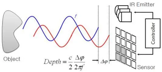
2. Time of Flight (ToF) / LiDAR
ToF emits modulated light pulses (direct ToF) or continuous waves (indirect/phase-shift ToF) and measures the round-trip time or phase difference for each pixel. It provides direct distance calculation, producing complete depth maps at video rates.
- Advantages: Works across a wide range of lighting conditions, independent of surface texture, fast acquisition, robust for dynamic scenes.
- Disadvantages: Higher hardware complexity and cost; multipath interference and limited resolution in some implementations.
Widely adopted in automotive LiDAR, smartphones, and industrial sensors. VCSEL arrays have become preferred illumination sources due to efficiency, eye safety, and beam quality.
3. Triangulation (Active)
Uses a known baseline between a light source (laser) and detector (camera) to calculate depth from the observed spot or line position via geometric relationships. It is highly accurate for specific measurement tasks and is common in industrial metrology, weld inspection, and aerospace applications but less common in consumer compact devices due to baseline size requirements.
Passive Ranging Methods
Passive techniques use ambient light and computational stereo or shape-from-X algorithms.
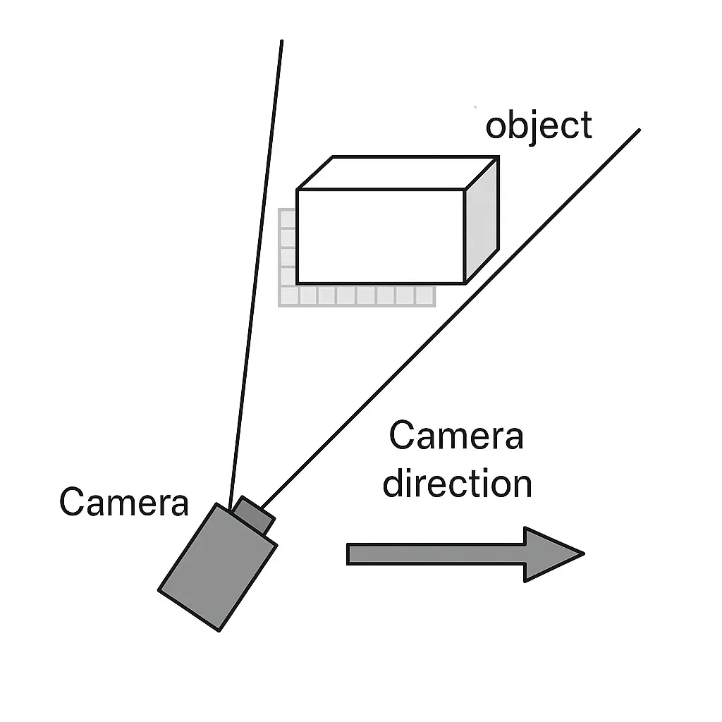
Monocular Vision
A single camera exploits focus/defocus cues, known object sizes, or motion parallax. While hardware is simple and low-cost, it generally offers lower accuracy without strong scene priors or machine learning assistance.
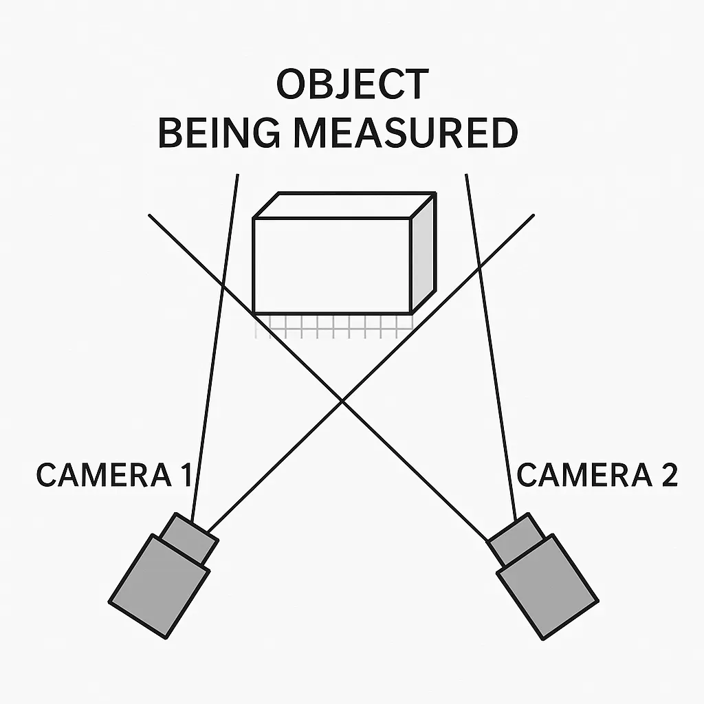
Stereo (Binocular) Vision
Two synchronized cameras separated by a baseline capture stereo image pairs. It computes a disparity map (pixel shifts between corresponding features) and applies triangulation for depth.
- Advantages: No active illumination needed, works well in textured environments.
- Disadvantages: Computationally intensive matching, sensitive to calibration, poor performance on low-texture surfaces, limited by baseline length.
Multi-View Vision
Extends stereo with additional cameras or sequential captures from moving viewpoints. It improves robustness, reduces ambiguities, and enhances accuracy through redundant measurements and multi-baseline matching.
Optoelectronic 3D Imaging Techniques and Sensor Technologies
Many commercial systems use indirect ToF with high-frequency modulation (tens of MHz) and phase detection on specialized sensors. Companies like SwissRanger and others have commercialized pixel arrays optimized for fast response and low noise.
Emerging single-chip approaches combine fast CMOS sensors with variable-focus elements (e.g., liquid lenses) for depth-from-focus/defocus. These enable compact modules that output both 2D images and depth maps without active projection in some modes, suitable for mobile and IoT devices.
Sensor Requirements include high-speed readout, low noise, high dynamic range, and the integration of analog processing and on-chip intelligence for real-time depth computation. MEMS components are often used for scanning or stabilization.
Applications Across Industries
3D vision applications are expanding rapidly:
- Consumer Electronics: Face unlock, portrait mode, AR experiences.
- Automotive: ADAS (object detection, distance estimation), surround view, in-cabin monitoring.
- Industrial & Robotics: Bin picking, dimensional inspection, navigation.
- Healthcare & Security: Biometrics, volumetric scanning, gesture interfaces.
Relevance to MEMS, Camera Modules, and PCB Design
MEMS technologies are integral for mirrors in scanning LiDAR or IMUs for stabilization. Camera modules integrate lenses, image sensors (CMOS), illuminators (VCSEL), and supporting electronics.
PCB Contributions:
- High-speed serial interfaces (MIPI CSI-2) for raw data transfer.
- Low-noise power domains for sensors and VCSEL drivers.
- Thermal vias and copper planes for heat dissipation from high-power illuminators.
- Shielding and grounding to control EMI in dense mixed-signal designs.
- Flex/rigid-flex for compact mechanical integration and alignment precision.
- Advanced manufacturing (HDI, controlled impedance, automated assembly) ensures high yield and reliability.
Precision PCB engineering is essential for maintaining signal integrity, power quality, and mechanical stability in high-performance 3D vision systems.
FAQ
Q1: What is the main advantage of ToF over structured light?
A1: ToF provides direct, fast depth measurement less sensitive to ambient light and surface texture.
Q2: How do liquid lenses contribute to 3D sensing?
A2: They enable rapid focal length changes for depth-from-focus techniques without mechanical movement.
Q3: Why are PCBs critical in 3D camera modules?
A3: They handle high-speed data, clean power delivery, thermal management, and EMI control while supporting compact, reliable integration of optical and electronic components.