 01:05
01:05
Silkscreen Errors
Silkscreen plays a critical role in printed circuit board design, providing essential markings such as component labels, polarity indicators, and assembly instructions that enhance usability and reduce errors during manufacturing and testing. However, silkscreen errors can introduce significant challenges, ranging from misaligned text and illegible markings to incorrect component outlines that lead to assembly mistakes or compliance issues. These problems often arise from design oversights, manufacturing tolerances, or material incompatibilities, potentially resulting in costly rework, production delays, or even functional failures in electronic devices. For engineers, designers, and hobbyists searching for solutions to silkscreen errors, understanding these issues is vital to ensuring high-quality PCB production and reliable end products. The Silkscreen Errors tag gathers a collection of in-depth articles that address common pitfalls and effective strategies for prevention and correction. Readers can find practical guidance on identifying issues like ink bleeding, resolution problems, or layer misalignment during the prototyping phase. For instance, best practices include optimizing artwork files with appropriate line widths and clearances, selecting compatible inks and substrates, and conducting thorough design rule checks before fabrication. These insights help mitigate risks in both low-volume prototypes and high-scale manufacturing, empowering users to improve board aesthetics, functionality, and overall yield rates. By delving into the resources under this tag, professionals can access case studies on real-world silkscreen troubleshooting, tips for software tools that automate error detection, and recommendations for collaborating with PCB manufacturers to achieve precise results. Whether you are refining a new design or diagnosing issues in an existing batch, these articles offer actionable steps to enhance your workflow and avoid recurring problems in future projects.
Video Guide
Technical Articles

How to Fix Via Tenting, Non-Plated Holes, and Silkscreen Issues in 6-Layer PCB CAM Review
Common HDI Gerber Design Mistakes Found During CAM Review
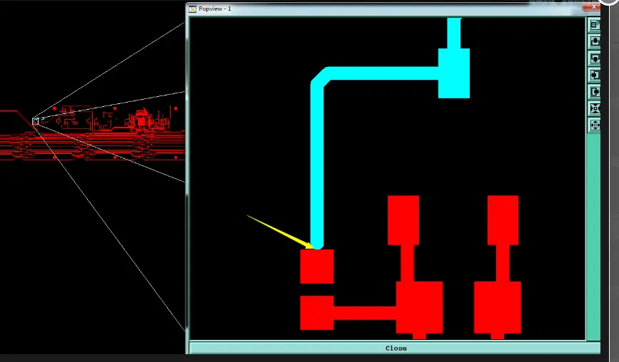
Avoid 4 Layer FR4 PCB Silkscreen and Solder Mask Production Errors
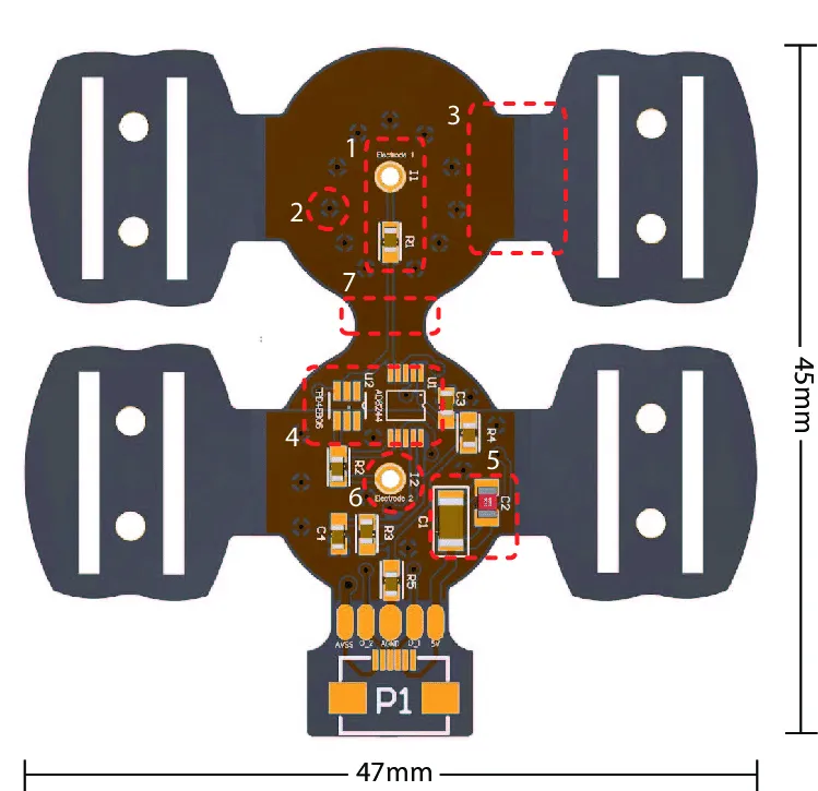
What Happens When FPC Characters Are Placed on or Too Close to Pads
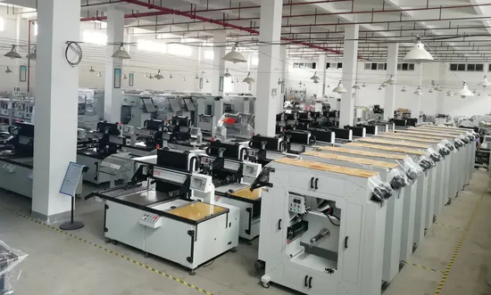
Why FPC Silkscreen Characters Keep Coming Out Blurry