










4 PCB Silkscreen Mistakes to Avoid for Reliable Production
What This Video Covers
This video addresses four frequent PCB silkscreen mistakes that routinely place orders on hold even after the design has passed DRC. Silkscreen (legend) that sits too close to pads can interfere with solder paste and component placement. Text that is too small or thin often breaks up during the actual printing process. Overlapping or poorly defined silkscreen layers create ambiguity for both fabricators and assembly technicians. Finally, solid outlines printed across dense copper or solder-mask features—especially around BGA packages—suffer from poor ink transfer and reduced readability.
The content is aimed at engineers and procurement teams preparing PCB prototype or production releases. It highlights the difference between DRC (design-rule compliance) and true DFM (design for manufacturability), showing why silkscreen must be checked against real process capabilities. Practical recommendations include minimum clearances, text dimensions used in standard fabrication, and preferred marking methods for high-density areas. These guidelines apply across rigid, multilayer, and HDI PCB designs and directly support higher first-pass yield in PCB assembly. Viewers leave with a concise pre-release checklist that reduces costly holds and re-spins.
Key Highlights
- Maintain at least 0.15 mm clearance between silkscreen and solderable pads to prevent assembly interference.
- Use minimum 0.75 mm text height and 0.1 mm line width for reliable ink transfer under standard processes.
- Replace solid outlines around BGA areas with four-corner marks and keep silkscreen layers free of overlaps or conflicting data.
Why Silkscreen Errors Still Stop Boards After DRC
Many engineering teams treat silkscreen as a low-priority layer once electrical and spacing rules are satisfied. In reality, silkscreen is a manufacturing feature that must survive the same process window as copper and solder mask. Fabricators apply legend ink after solder-mask curing; the ink must wet properly, cure without cracking, and remain legible after subsequent handling and cleaning. When silkscreen violates process limits, the board is flagged at CAM or during first-article inspection—often after the customer has already waited for DRC clearance.
This mismatch between "design rules" and "process capability" is the core reason orders are placed on hold. DRC tools typically check only geometric clearance and layer presence. They do not simulate ink viscosity, screen-mesh limitations, or the interaction between silkscreen and underlying topography. Experienced manufacturers therefore run a separate DFM review focused on legend printability. Catching these issues before Gerber release protects both schedule and cost, especially on PCB mass production runs where a single silkscreen revision can delay an entire lot.
Detailed Breakdown of the Four Critical Silkscreen Mistakes
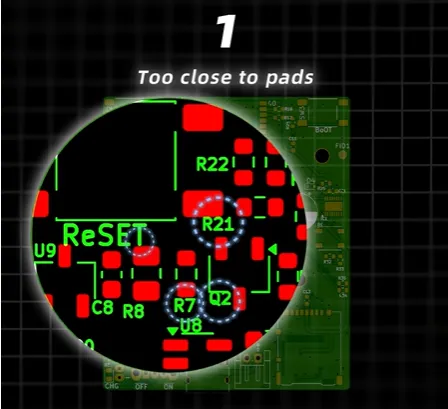
Mistake 1: Silkscreen Too Close to Pads
Silkscreen ink that encroaches on solderable surfaces can contaminate the pad, reduce solder-wetting area, or create solder-mask dams that trap flux. Most fabricators require a minimum clearance of approximately 0.15 mm between the edge of any silkscreen feature and the nearest copper pad or exposed metal. Tighter clearances may be accepted on specialized processes, but the standard 0.15 mm rule covers the majority of rigid and multilayer boards. Violation usually triggers a customer query or automatic hold.
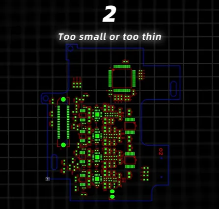
Mistake 2: Text Height and Line Width Below Process Limits
What appears crisp on a high-resolution monitor frequently fails on the production floor. Thin lines and small characters break up because the screen mesh cannot hold sufficient ink or because the ink itself is sheared during printing. For AIVON's standard process the practical minimums are 0.75 mm character height and 0.1 mm line width. Smaller text is possible with specialty fine-pitch screens, but it increases cost and risk. Always verify the manufacturer's published capability rather than relying on CAD default fonts.
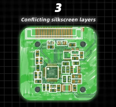
Mistake 3: Conflicting or Overlapping Silkscreen Layers
Multiple silkscreen layers (top, bottom, or auxiliary) that contain duplicate or contradictory markings force the fabricator to guess which data set is intentional. Overlapping text, reference designators printed on top of polarity marks, or residual construction lines left in the Gerber files all create ambiguity. Clean, single-purpose silkscreen layers with clear hierarchy eliminate interpretation errors and reduce the chance of missing or duplicated markings on the finished board.
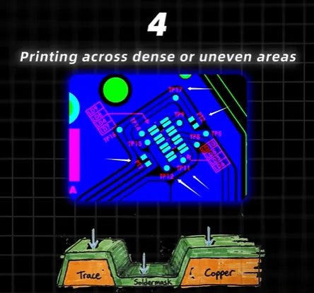
Mistake 4: Printing Across Dense or Uneven Surfaces
Underlying copper features, solder-mask dams, and via tenting create local height variations that disrupt uniform ink transfer. Solid rectangular outlines around dense component groups—especially BGA packages—are particularly problematic. Ink tends to thin or skip over raised areas, leaving incomplete or illegible marks. Replacing solid outlines with four discrete corner marks improves both print quality and visual clarity for assembly operators.
Practical Silkscreen DFM Guidelines and Clearance Table
The following table summarizes the key process limits used by many mid-to-high-volume fabricators. Always confirm the exact values with your chosen manufacturer, as capabilities vary with equipment and ink chemistry.
| Parameter | Recommended Minimum | Typical Risk if Violated | Notes |
|---|---|---|---|
| Silkscreen-to-pad clearance | 0.15 mm | Solder contamination, assembly defects | Measured from ink edge to copper edge |
| Character height | 0.75 mm | Broken or illegible text | Measured on finished board |
| Line / stroke width | 0.1 mm | Incomplete printing, cracking | Applies to both text and graphics |
| Silkscreen-to-board-edge | 0.3–0.5 mm | Ink bleed or edge damage | Depends on scoring / routing process |
| Overlap between silkscreen features | None | Ambiguous or missing marks | Clean layer hierarchy required |
These values form a practical pre-release checklist. Incorporating them into your CAD design rules or a simple DFM script dramatically reduces the probability of silkscreen-related holds.
Silkscreen Design Recommendations for High-Density and BGA Boards
On high-density interconnect and fine-pitch assemblies the available real estate for legend is limited. Prioritize essential information—reference designators, polarity marks, and critical warning symbols—and omit decorative or redundant text. For BGA and similar area-array packages, four-corner marks plus a single pin-1 indicator provide sufficient orientation without crowding the package footprint. When boards will be used in medical, automotive, or industrial control environments, ensure that all markings remain legible after conformal coating or additional cleaning processes.
Finally, treat silkscreen as a living manufacturing layer rather than a static documentation layer. Review it with the same rigor applied to copper and solder-mask data. Doing so converts a frequent source of production friction into a reliable contributor to first-pass yield.
FAQ
Q1: What minimum silkscreen-to-pad clearance do most fabricators require?
A1: Most standard processes require approximately 0.15 mm clearance between the edge of any silkscreen feature and the nearest solderable pad. Tighter clearances may be possible with specialized equipment but should be confirmed in advance to avoid holds.
Q2: Why is 0.75 mm the typical minimum text height for PCB silkscreen?
A2: Below this height, characters frequently break up or become illegible during screen printing because of mesh limitations and ink rheology. 0.75 mm height combined with 0.1 mm stroke width provides reliable results under common process conditions.
Q3: How should silkscreen be marked around BGA packages?
A3: Solid outlines often print poorly over the dense copper and via features beneath a BGA. Four discrete corner marks plus a clear pin-1 indicator deliver better ink transfer and clearer orientation for assembly operators.
Q4: Can overlapping silkscreen layers cause a board to be rejected?
A4: Yes. Conflicting or duplicated data forces the fabricator to interpret intent, increasing the risk of missing or incorrect markings. Clean, non-overlapping layers eliminate this ambiguity.
Q5: Does silkscreen design affect SMT assembly yield?
A5: Incorrect clearance or poorly printed polarity marks can lead to component misorientation, solder contamination, or inspection failures, all of which reduce first-pass assembly yield.
Spent hours getting your PCB through DRC — only to have the order put on hold?
Your silkscreen might be the problem.
Here are four mistakes to check before production.
One. Too close to pads.
Silkscreen over solderable areas can interfere with assembly.
Keep enough clearance — around 0.15 mm can be required, depending on the process.
Two. Too small or too thin.
What looks sharp on screen can break up during printing.
For AIVON's standard process, we generally recommend at least 0.75 mm text height and 0.1 mm line width .
Three. Conflicting silkscreen layers.
Overlapping or unnecessary markings can leave engineers guessing what you actually want printed.
Keep your silkscreen layers clean and clearly defined.
Four. Printing across dense or uneven areas.
Underlying copper and solder mask features can affect ink transfer.
And around BGA areas, solid outlines may be better replaced with four corner marks.
DRC checks your design.
DFM checks whether it can actually be made.
This is AIVON.
Check this before your next layout.





