


3 PCB Design Mistakes That Quietly Increase Your Costs
What This Video Covers
This video delivers actionable insights for engineers and procurement teams focused on reducing PCB costs through smarter design rather than simply negotiating lower quotes. It highlights three common PCB design mistakes that drive up fabrication expenses: overly tight tolerances on non-critical features, selection of premium or non-standard materials when standard options suffice, and suboptimal panelization that wastes material and lowers production efficiency.
By addressing these issues early in the design phase, manufacturers can achieve significant savings on rigid PCBs, flexible circuits, and multilayer boards while maintaining reliability for demanding applications like automotive electronics, industrial control systems, and IoT devices. The content emphasizes Design for Manufacturability (DFM) principles that balance performance, reliability, and cost.
Viewers learn why the cheapest PCB supplier quote often fails to deliver the lowest total cost, especially when design choices trigger higher scrap rates, longer lead times, or additional processing steps during PCB fabrication, drilling, plating, and assembly. Practical recommendations help teams optimize layer stack-up, material selection, and layout for better yields.
Whether developing prototypes or preparing for mass production, these strategies support cost-effective decisions across FR4-based boards and more specialized constructions.
For instant pricing feedback on optimized designs, use our PCB online quote tool. Teams needing assembly services can also explore PCBA quote options, while flex projects benefit from dedicated flexible PCB quote guidance.
Key Highlights
- Tolerances drive costs: Unnecessary tight tolerances increase precision requirements in etching, drilling, and plating, raising scrap rates and cycle times.
- Material choices matter: Defaulting to standard FR4 and common finishes (like HASL or ENIG) reduces sourcing complexity and material premiums without sacrificing performance in most applications.
- Panelization efficiency: Optimized layouts maximize panel utilization, lowering per-board material waste and improving overall manufacturing throughput.
Why Smart PCB Design Beats Hunting for the Cheapest Quote
Many OEMs focus exclusively on supplier pricing, but experienced teams know that design-stage decisions have a far greater impact on final PCB costs. Poor DFM choices can increase fabrication expenses by 20-50% through higher material usage, slower production speeds, and quality issues that require rework.
Factory data consistently shows that designs reviewed with manufacturers early in the process achieve better yields and lower total ownership costs. This is especially true for multilayer PCBs and projects transitioning from prototype to volume production.
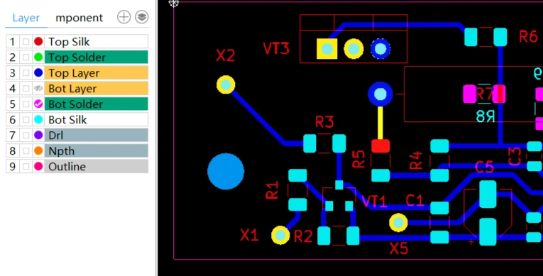
Mistake 1: Over-Specifying Tight Tolerances
Specifying ±0.05mm trace width/spacing or ultra-tight hole tolerances when your application only needs ±0.1mm dramatically raises costs. Tighter features demand slower etching speeds, more precise drilling, additional inspection, and lower panel yields.
Practical Recommendation: Review your schematics against actual electrical and mechanical needs. Relax non-critical dimensions to standard capabilities. This often reduces drilling and plating steps significantly.
Failure case: A medical device client reduced costs by 28% simply by adjusting tolerance callouts on non-impedance-controlled layers.
Mistake 2: Choosing Non-Standard Materials Unnecessarily
While Rogers or high-Tg materials excel in RF and thermal-heavy designs, using them for general-purpose boards inflates costs due to higher raw material prices and longer lead times. Standard FR4 performs reliably in most consumer electronics, industrial control, and automotive applications below certain temperature thresholds.
DFM Tip: Default to FR4 unless signal integrity, thermal management, or environmental requirements demand otherwise. Consult with your manufacturer on stack-up options that balance performance and price.
Mistake 3: Inefficient Panelization and Layout Decisions
Poor panelization leads to excessive material waste and higher per-unit pricing. Factors like board shape, fiducials, tooling holes, and array configuration directly affect how many boards fit on a standard production panel.
Best Practice: Work with your fabricator to define optimal panel sizes early. Use v-scoring or tab-routing strategically and minimize unused space. This is critical when scaling to PCB mass production.
Real-World Cost Impact and DFM Best Practices
Implementing these changes typically yields 15-40% savings depending on volume and complexity. Key actions include running DFM checks before release, engaging manufacturers during the design phase, and documenting cost drivers in your bill of materials review.
Design Factor Comparison
| Design Factor | Costly Approach | Cost-Effective Alternative | Typical Savings |
|---|---|---|---|
| Trace/Space Tolerance | ±0.05mm everywhere | ±0.1mm for non-critical | 15-25% |
| Material Selection | Rogers for all layers | FR4 with selective high-frequency | 20-35% |
| Panel Utilization | Single boards or poor array | Optimized multi-up with v-score | 10-30% |
| Surface Finish | Premium ENIG on all | HASL where appropriate | 5-15% |
FAQ
Q1: How much can better PCB design reduce manufacturing costs?
A1: Smart DFM adjustments on tolerances, materials, and panelization commonly deliver 15-40% savings, often exceeding what price negotiation alone can achieve, especially at prototype and mid-volume runs.
Q2: When should I choose standard FR4 versus premium materials?
A2: Use standard FR4 for most applications under 130°C with moderate signal speeds. Reserve Rogers, high-Tg, or metal-core materials for high-frequency, high-power, or extreme environment needs to control costs effectively.
Q3: Does tight tolerance always increase PCB price significantly?
A3: Yes—tighter tolerances reduce yield, slow production, and require advanced process controls. Relaxing non-critical features is one of the fastest ways to lower costs without affecting functionality.
Q4: How does panelization affect PCB assembly pricing?
A4: Efficient panelization increases the number of boards per panel, reducing material waste and setup time, which lowers both fabrication and SMT assembly costs.
Q5: What is the best time to review designs for cost optimization?
A5: Before finalizing gerbers—ideally during the schematic and layout phase. Early collaboration with your manufacturer prevents expensive revisions later.
Trying to reduce PCB costs?
Don't start by choosing the cheapest supplier.
Start with your design.
First, avoid unnecessary tight tolerances. If your application doesn't require ultra-fine features, keeping specifications reasonable can significantly reduce manufacturing costs.
Second, use standard materials whenever possible. Standard FR-4 and common surface finishes are usually more affordable and easier to source.
Third, optimize your panelization. Better panel utilization means less wasted material and more efficient production.
Here's the key:
The cheapest PCB isn't always the lowest-cost PCB.
In many cases, smart design decisions save more money than negotiating a lower quote.
Which cost-saving method has worked best for you?





