 00:51
PCB Cost Reduction
In the competitive landscape of electronics manufacturing, achieving PCB cost reduction is essential for engineers, designers, and procurement specialists aiming to balance budget constraints with high-quality outcomes. This tag, PCB Cost Reduction, gathers a curated collection of articles focused on proven strategies to minimize expenses throughout the printed circuit board lifecycle, from initial design to final assembly. Whether you are optimizing prototypes for startups or scaling production for established firms, these resources address common pain points such as material selection, layout efficiencies, and supplier negotiations. Understanding the factors that drive PCB costs empowers you to make informed decisions that enhance profitability. For instance, selecting cost-effective substrates like FR-4 over premium alternatives can significantly lower material expenses without sacrificing performance in standard applications. Design best practices, such as minimizing layer counts, optimizing trace widths, and incorporating panelization techniques, further reduce fabrication and assembly fees. Volume-based approaches, including just-in-time manufacturing and bulk purchasing, offer additional savings, while evaluating overseas versus domestic suppliers helps navigate trade-offs in lead times and tariffs. Professionals searching for PCB cost reduction often seek practical tools to implement these ideas. Our articles delve into real-world case studies, where techniques like design for manufacturability (DFM) have slashed costs by up to 30 percent in high-volume runs. You will find guidance on leveraging software tools for simulation and cost estimation, ensuring your projects stay within budget. As you browse the tagged content, consider how these insights apply to your specific challenges, whether refining a single-board design or overhauling a supply chain. This collection serves as a valuable reference for sustaining innovation while controlling expenditures in the fast-evolving electronics sector.
Video Guide

Technical Articles
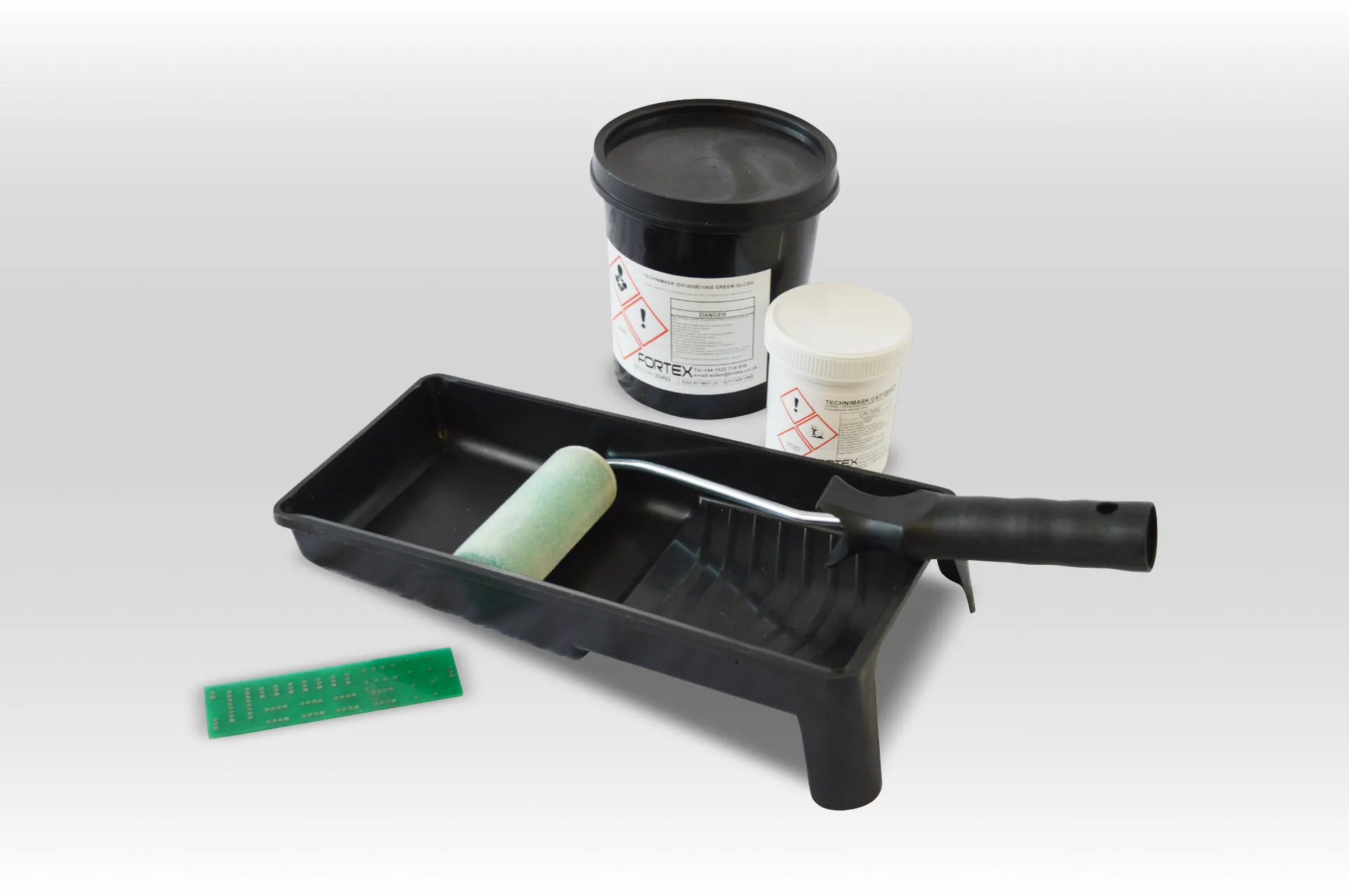
Liquid Photoimageable Resist for PCB Pattern Transfer: Process, Controls, and Practical Tips
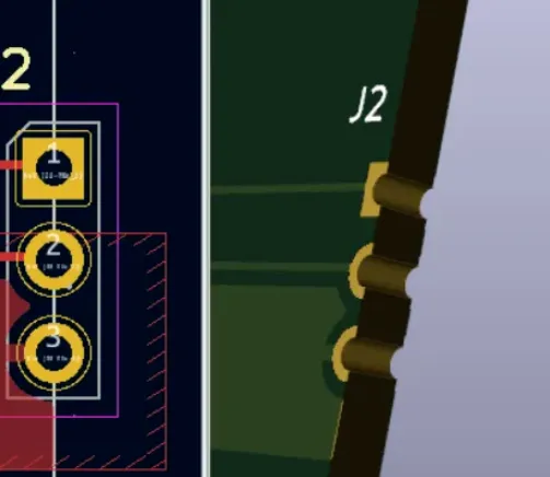
Designing PCB Castellated Holes with KiCad
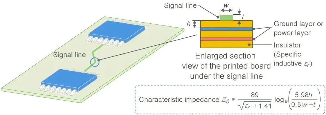
Revealing the "Pseudo Eight-Layer" Stackup: Can a Six-Layer PCB Deliver Eight-Layer Performance?
Embedded Resistors and Capacitors in PCB Manufacturing
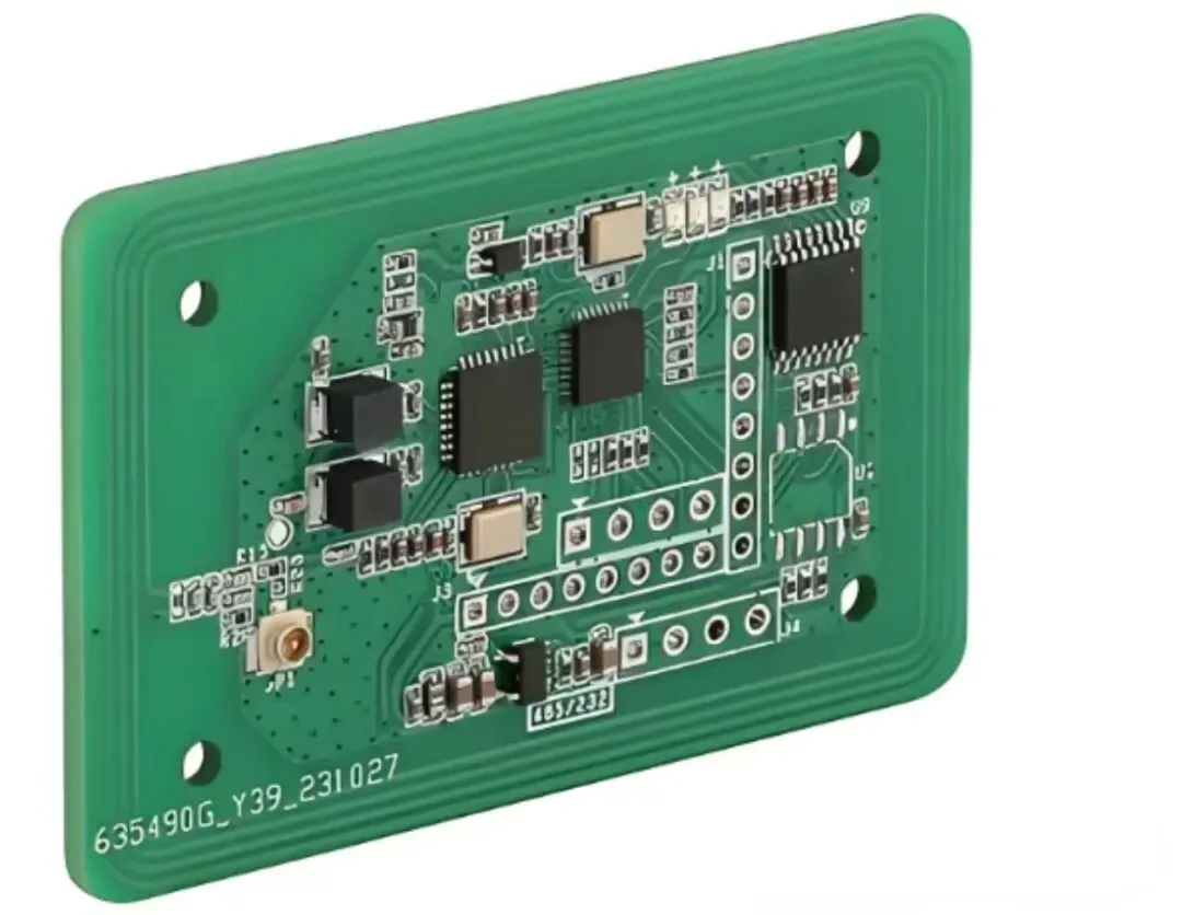
Using PCB Traces to Replace Fuses for Cost Reduction: How Many Risks Are Hidden?
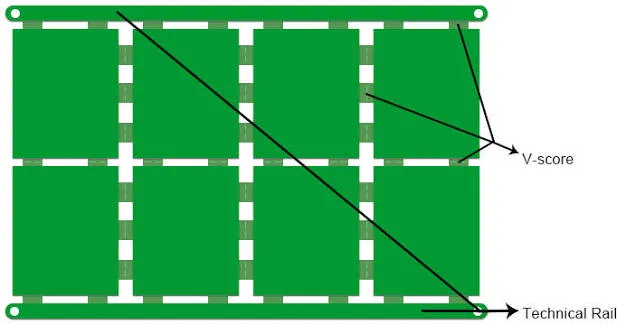
Why PCB Panels and Edge Rails Are Used in PCB Manufacturing

4 Layer vs 6 Layer PCB: Which One Should You Choose?

Single Layer and Multilayer PCB: Key Differences in Design and Applications

6 Layer vs 8 Layer PCB: Key Differences and Cost Comparison

PCB Panelization Design Optimization and Practical Considerations
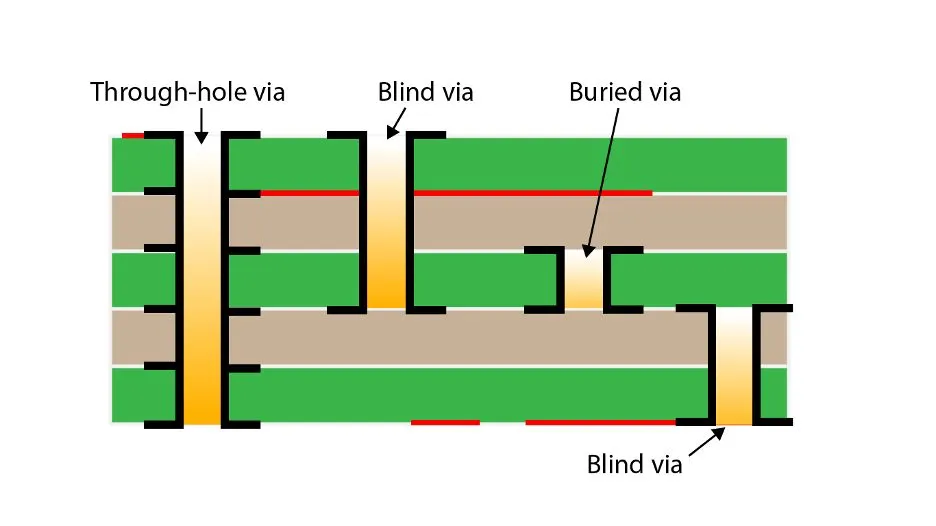
PCB Design Using Blind or Buried Vias Could Lower Fabrication Costs
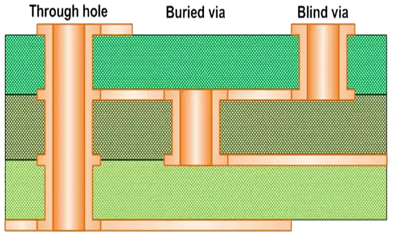
Cost Effective Buried Via Implementation: Balancing Performance and Price

HDI PCB Cost: Manufacturing Factors and Cost-Effective Design Strategies
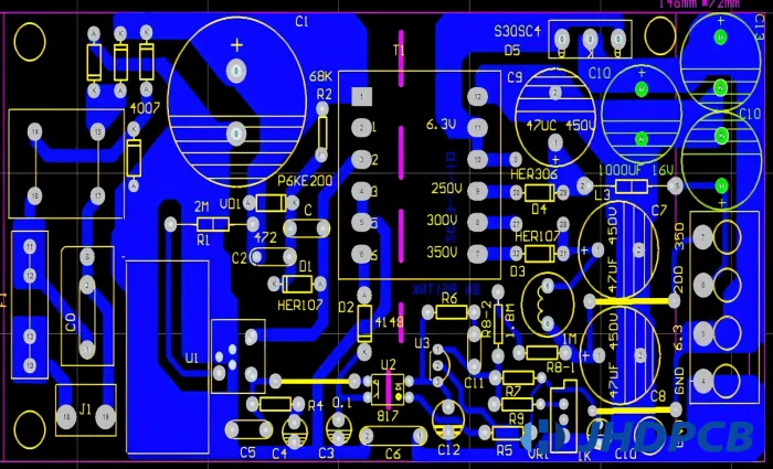
Cost Effective PCB Trace Routing: Strategies for Reducing Manufacturing Costs

Advantages of Single-Chip Bluetooth Solutions
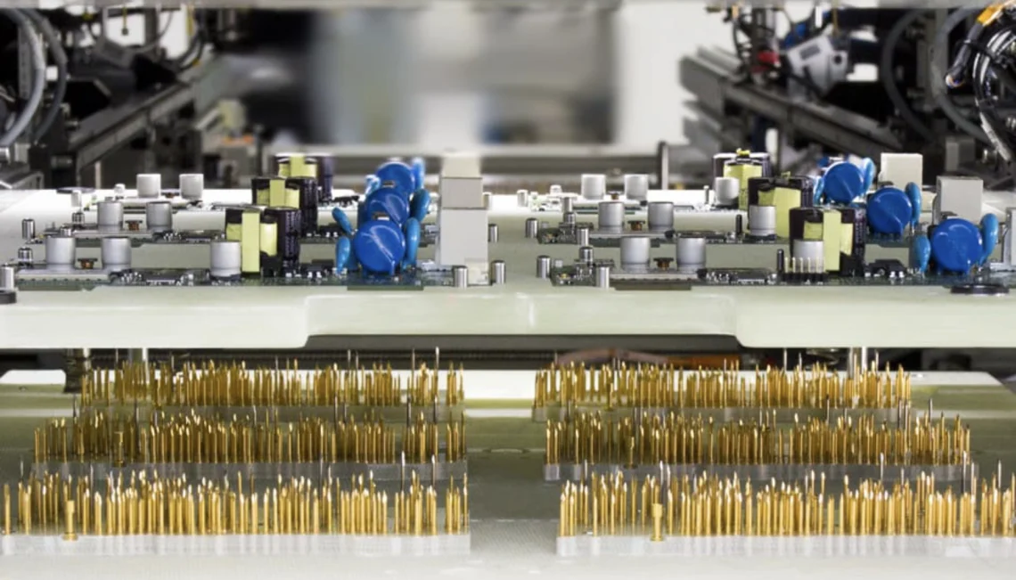
Cutting Costs with DFT: Optimizing Test Strategies for Electronic Products
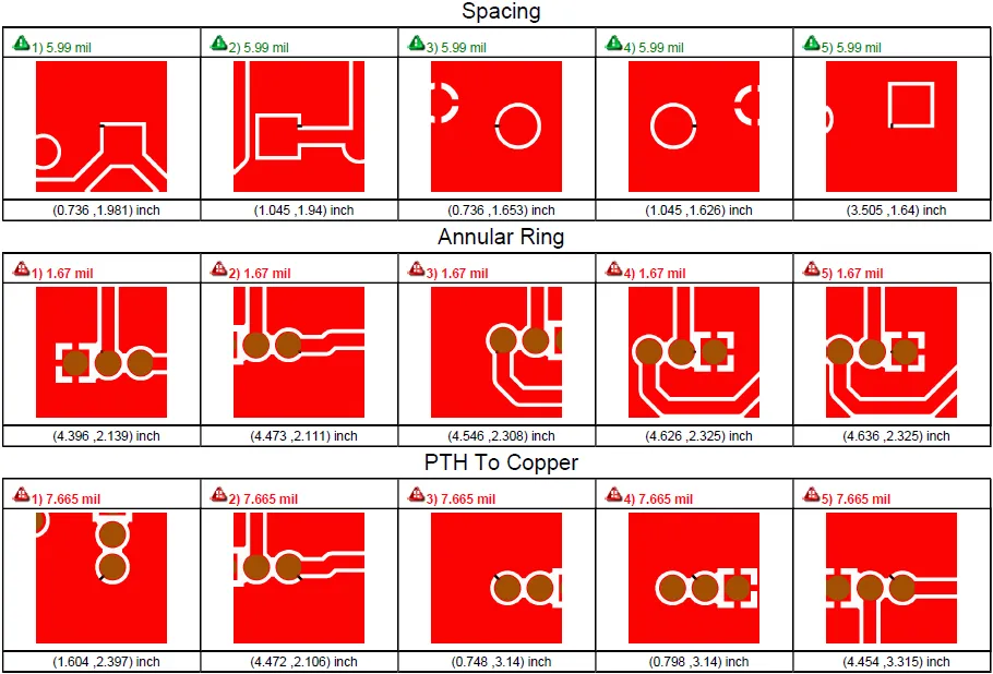
Unlocking Cost Savings: A Deep Dive into PCB DFM Review
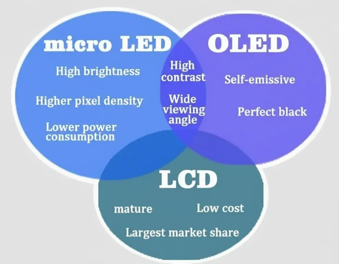
TFT LCD, OLED, and Micro LED: display principles

RF Front-End Growth Drivers and Market Outlook